Research team advances understanding of atomically thin crystal growth
(Phys.org) —UT's College of Engineering has made recent headlines for discoveries that, while atomically small, could impact our modern world.
The Proceedings of the National Academy of Sciences, the official scientific journal of the organization, recently published an interdisciplinary study led by Department of Electrical Engineering and Computer Science associate professor Gong Gu.
Gu's team—which included professor Gerd Duscher from the Department of Materials Science and Engineering and students from both engineering and the Department of Physics—focused on the role of epilayer-substrate interactions in determining orientational relations in van der Waals epitaxy.
In rudimentary terms, the study looked at growing an atomically thin, or two-dimensional, crystal—the epilayer—on top of a substrate. The substrate can be a bulk, or three-dimensional, crystal or another two-dimensional crystal.
"Conventional epitaxy is like stacking Lego blocks," said Gu. "The studs and cylinders are rigid and therefore must be matched very well. The covalent bonding between a three-dimensional epilayer and a 3D substrate is just like that."
"Now imagine Lego pieces with flexible studs and cylinders, which do not have to interlock exactly but just weakly interact and you have an idea of what van der Waals epitaxy is."
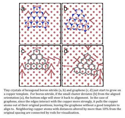
It was with those van der Waals "blocks" that Gu's team made its surprising discovery: The weakly interacting pairs tend to orientationally align to each other, in some ways better than the more strongly bonded pairs.
The team conducted its research with 2D crystals of graphene and hexagonal boron nitride, as graphene interacts more strongly with the substrate but does not always align with it, while hexagonal boron nitride strictly aligns.
The edges of the 2D crystals "steer" their growth at the very beginning. The stronger edge-substrate interaction distorts the atoms' positions in the substrate, leaving the 2D crystal no good template to align to.
"That was somewhat surprising," said Gu. "The supposition that most people had going into this was that the materials with the strongest bonds would have the most predictable, most orderly growth, but that was proven to not always be the case."
In fact, this knowledge led to another recent advance in 2D crystal growth, where graphene and boron nitride are joined in-plane, with the zipperlike locking between the two overriding the soft studs. That advance, in turn, spawned yet another discovery—the observation of "boundary states" at the boundary.
More information: "Unusual role of epilayer–substrate interactions in determining orientational relations in van der Waals epitaxy." PNAS 2014 ; published ahead of print November 10, 2014, DOI: 10.1073/pnas.1405613111
Journal information: Proceedings of the National Academy of Sciences
Provided by University of Tennessee at Knoxville


