Improving printed electronics process and device characterization
. The defect is visible as a dark feature at the boundaries of two sequentially deposited, i.e. stacked thin film layers. Credit: Advantech US/MCL")
Advantech US, Inc. is a Pittsburgh-based technology company that uses a green additive manufacturing shadow mask process to build electronics and fine-line conductors by deposition of vaporized bulk materials – such as metals – onto various rigid and flexible substrates. By building up components layer by layer, Advantech is able to create complex devices with features in the size range of 3–50 micrometers, filling an important size gap between nanoscale lithography and printed circuit board manufacturing, with significant cost benefits, broad design flexibility, simpler processing steps, and reduced material use. Their products include active matrix display backplanes for ePaper and OLED displays.
In Penn State's Nanofabrication Laboratory, etch and deposition lead Guy Lavallee, working with research and development engineer Chad Eichfeld and lithography process engineer Michael Labella, successfully fabricated a prototype mask of silicon etched with the required micrometer-scale features. A second prototype with fine alignment features is being developed.
Advantech's evaporation process can deposit metals, dielectrics, and semiconductors using the miniLineTM, an in-line multi-chamber vacuum deposition system. At times, however, unexpected particle contamination
affects the performance of the deposited micrometer-sized electronic devices. Vince Bojan and Julie Anderson in the Materials Characterization Laboratory are using the scanning electron microscope and a scanning Auger Electron Spectrometer to identify the chemical elements in the contaminants and thus pinpoint the source of such yield-limiting defects. Together, the two labs are helping a Pennsylvania company expand into the highly competitive microelectronic devices and circuitry market with a simpler, more economical process.
Advantech Senior Scientist Volker Heydemann had this to say about working with MRI: "It's extremely helpful to identify the chemistry of the contaminants on our products. Vince Bojan and Julie Anderson in the Materials Characterization Lab had useful results in just a couple of days. They are real experts in electron microscopy and spectroscopy. The opportunity to apply Nanofab's processing capabilities with MCL's advanced materials characterization techniques and expertise provides insights in our process beyond the capabilities of our in-house suite of test and quality assurance tools. Our project with Penn State helped identify and improve critical steps in our manufacturing process."
-
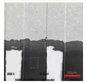
A secondary electron image acquired with the AES (Auger) instrument. These images were used to select regions for compositional analysis – one example is the box that shows a sample area for Auger spectroscopy. Credit: Advantech US/MCL -
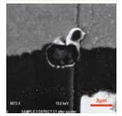
SEM image of defect at higher magnification in the AES instrument used to determine the local elemental composition. Credit: Advantech US/MCL
Provided by Pennsylvania State University


