Next-generation device enabling improved smartphone battery life and high definition in televisions

A research by Japan's NIMS International Center for Materials Nanoarchitectonics has succeeded in developing a metal oxide film transistor using a material with an unique atomic composition.
Metal oxide film transistors are an object of research and technical development as next-generation materials for amorphous silicon transistors, which are used to switch picture elements (pixels) in the flat panels of existing televisions, computers, smartphones, and similar products. In current displays using amorphous silicon transistors, power consumption is increasing rapidly due to new high resolution and touch panel features. As there are limits to improvement of the properties of the conventional material, new materials are considered necessary as an alternative to amorphous silicon thin films.
In recent years, it has been found that IGZO film transistors, which are produced from a mixed target obtained by oxidizing indium, gallium, and zinc, operate with high electron field effect mobility. Although process development is underway aiming at development to practical applications, control of oxygen and moisture is extremely difficult with this material. Therefore, development of techniques for controlling these factors had become an issue for production of transistors using a metal oxide film as a semiconductor thin film. To solve this problem, materials that enable transistor operation with novel metal oxide films consisting of easily-handled atoms had been the object of an ongoing search.
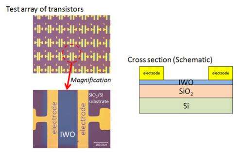
In this research, an IWO (indium-tungsten oxide) thin film that operates as a thin film transistor was developed by adding an extremely small amount of tungsten oxide to indium oxide. The developed material does not contain gallium or zinc, which are elements that are difficult to control in an amorphous state. Because a homogeneous amorphous film can be produced simply by sputter film-forming at low energy, without heating the substrate or similar operations, thin films are easily formed with this new material, and operation as a transistor with high characteristics is possible, even using a structure without a protective film with an unprecedented thin film thickness of 10nm. In addition to avoiding use of expensive gallium, the thin structure is also effective in reducing material costs because the total amount of raw materials used in the thin film can be reduced, and also enables high production efficiency.
This achievement will be effective in realizing low power consumption in displays, which are a source of high power consumption in smartphones, thereby responding to an important need in a field that is currently enjoying explosive growth. It is also expected to be an effective technology for frequency improvement, which is essential for higher resolution in televisions.
Provided by National Institute for Materials Science


