World-leading microscopes take candid snapshots of atoms in their 'neighborhoods'

We can directly see the hidden world of atoms thanks to electron microscopes, first developed in the 1930s. Today, electron microscopes, which use beams of electrons to illuminate and magnify a sample, have become even more sophisticated, allowing scientists to take real-world snapshots of materials with a resolution of less than half the diameter of a hydrogen atom.
Now, scientists at the Department of Energy's Lawrence Berkeley National Laboratory (Berkeley Lab) are pushing the boundaries of electron microscopy even further through a powerful technique called 4-D-STEM, a term that stands for "2-D raster of 2-D diffraction patterns using scanning transmission electron microscopy."
Their findings, reported in Nature Communications and Nature Materials, show for the first time how 4-D-STEM can provide direct insight into the performance of any material—from strong metallic glass to flexible semiconducting films—by pinpointing specific atomic "neighborhoods" that could compromise a material's performance, or perhaps have the potential to improve it.
"Historically, electron microscopes have been most useful at high resolution for imaging hard materials," said author Andew Minor, who led the studies. Minor is the facility director for the National Center for Electron Microscopy (NCEM) at Berkeley Lab's Molecular Foundry; a member of the Materials Sciences Division at Berkeley Lab; and a professor of materials science and engineering at UC Berkeley.
"Now, in these studies, we've shown that when 4-D-STEM is deployed with our high-speed detectors, customizable algorithms, and powerful electron microscopes, the technique can help scientists map out atomic or molecular regions in any material—even beam-sensitive, soft materials—that weren't possible to see with previous techniques," he said.
Mapping out atomic neighborhoods in soft materials

In the field of flexible electronics and organic photovoltaics, scientists typically use X-rays to characterize a material's molecular structure because the electron beam in an electron microscope would destroy the material.
"But X-rays can't be focused to the size of single atoms," said Minor. "When it comes to reaching atomic resolution, nothing beats electrons. You can focus electrons to a very small point, and the electrons react very strongly with materials. That's good if you want a lot of signal, but it's bad if you have a beam-sensitive material."
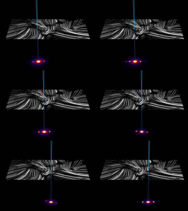
In their Nature Materials study, Minor and co-authors demonstrated how high-speed detectors that capture atoms in action at up to 1,600 frames per second with 4-D-STEM allowed unprecedented molecular movies of a small-molecule organic semiconductor. The movie showed how the molecular ordering in the semiconductor, often used in organic solar cells, changed in response to a common processing additive (called DIO or 1,8-diiodooctane) that is known to enhance solar cell efficiency.
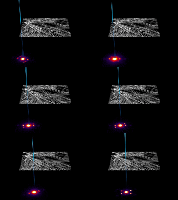
In conducting the Nature Materials study as part of DOE's Soft Matter Electron Microscopy and Scattering program, the 4-D-STEM experiments allowed Minor and his co-authors to map out the orientation of the grains of ordered molecules within the material, which look like intersecting, overlapping roads connecting adjacent neighborhoods.
Such details, which are not possible to observe with conventional STEM, are significant because low-angle boundaries—like long, straight tunnels through which a car can accelerate unimpeded at high speed—are necessary for electrons to couple and generate a charge in a functional semiconductor.
Using this powerful new technique, the researchers clearly demonstrated that the DIO additive dramatically alters the material's nanostructure, and that this overlapping grain structure is key to the enhanced efficiency observed in solar cells made from these materials, explained Colin Ophus, a research scientist at NCEM.

"The reason why it's important to see orientation distribution of a material is because these boundaries strongly mediate the material's electrical conductivity," he said. "If an electron hits a wall or a grain boundary it has a high chance of bouncing off, which compromises its performance."
Building better materials, atom by atom
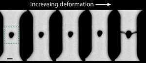
In their Nature Communications study, carried out as part of DOE's Mechanical Behavior of Materials program, Minor, Ophus, and co-authors used 4-D-STEM to pinpoint atomic-scale "weak links" in bulk metallic glass that ultimately lead to fractures under stress.
Regular metals are crystalline materials, which means that their atoms are arranged in a perfect, repeating pattern—like tennis balls perfectly stacked inside a cube so that they fill up the space. When an atom is missing such a defect is obvious under an electron microscope, making it easier to predict where a material might be compromised.
But bulk metallic glasses (BMGs) are amorphous, meaning that their atoms form a disordered pattern—like a randomly assembled, unstable pile of tennis balls, golf balls, and baseballs tossed inside a box. And this unpredictable structure is what makes it hard for materials scientists to figure out where those atomic defects might be hiding as they compromise a material's toughness.
By using 4-D-STEM with high-speed electron detectors, the researchers measured the average spacing between atoms within certain regions of the BMG material, and recorded the "strain" or change in this spacing as the material is pulled until it breaks.

They showed that 4-D-STEM, when combined with high-speed electron detectors and fast algorithms to analyze hundreds of thousands of diffraction patterns throughout a sample, can identify the precursors in the material's atomic structure that cause it to fail, Ophus said.
Focusing on the future of 4-D-STEM
At the heart of this marriage between high-speed detectors and 4-D-STEM microscopes are finespun algorithms, which Ophus customizes for every user running 4-D-STEM experiments at the Foundry's NCEM facility.
"We run some of the fastest 4-D-STEM simulation codes in the world, and each user project at the Foundry brings unique challenges, requiring measurements of different materials' properties from many different samples," said Ophus. "But we know that not everyone can write code, so we help our users by developing custom-written, user-friendly software that allows them to simulate and model real-world materials at these unprecedented scales."
Ophus added that users can benefit from their customized scripts even without coming to Berkeley Lab. He and Minor, in collaboration with researchers from Berkeley Lab's Computational Research Division and the Toyota Research Institute, are developing an open-source, Python-based software so that the power of 4-D-STEM is available to hundreds of institutions instead of just a handful.
Once completed, their open source software, coupled with Berkeley Lab's new ultrafast 4-D Camera, will pave the way for the imaging of materials at the atomic or molecular level as they morph in response to stress at an even higher resolution and faster speed, said Minor. This camera is currently the fastest electron detector in the world, capturing atomic snapshots at 87,000 frames per second: about 50 times faster than the current state of the art.
More information: Thomas C. Pekin et al. Direct measurement of nanostructural change during in situ deformation of a bulk metallic glass, Nature Communications (2019). DOI: 10.1038/s41467-019-10416-5
Ouliana Panova et al. Diffraction imaging of nanocrystalline structures in organic semiconductor molecular thin films, Nature Materials (2019). DOI: 10.1038/s41563-019-0387-3
Journal information: Nature Communications , Nature Materials
Provided by Lawrence Berkeley National Laboratory


