September 24, 2019 feature
Quantum Hall-based superconducting interference device

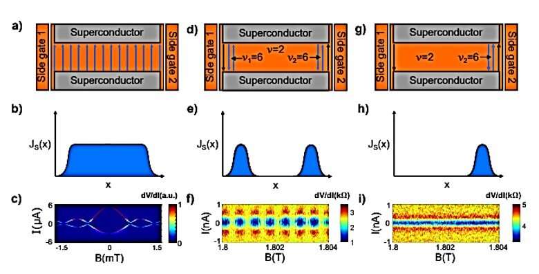
In a recent report published on Science Advances, Andrew Seredinski and co-workers presented a graphene-based Josephson junction with dedicated side gates fabricated from the same sheet of graphene as the junction itself. The interdisciplinary research team in the departments of physics, astronomy and advanced materials in the U.S. and Japan found the side gates to be highly efficient, allowing them to control carrier density along either edge of the junction across a wide range of magnetic fields. For example, they populated the next Landau level (where the number of electrons are directly proportional to the strength of the applied magnetic field) within magnetic fields in the 1 to 2-Tesla (T) range, to result in quantum Hall plateaus. Then when they introduced counter-propagating quantum Hall edge states along either side of the device, they observed a supercurrent localized along the edge of the junction. In the present work, they studied these supercurrents as a function of magnetic field and carrier density.
In quantum mechanics, physicists classify particles either as fermions or bosons. This classification is crucial to understand a variety of physical systems including lasers, metals and superconductors. Interactions between electrons or atoms in some two-dimensional (2-D) systems can lead to the formation of quasi particles that break from the fermion-boson dichotomy; to form 'non-Abelian' states of matter. Many experimental studies attempt to identify non-Abelian states in systems that manifest the quantum Hall (QH) effects (quantization of resistance in two-dimensional electronic systems). The identification of such states will be useful for quantum computation.
Physicists predict the interplay of spin-helical states and superconductivity to allow access to non-Abelian excitations such as Majorana Zero modes (MZM). These states may form the basis for quantum computing architectures, which take advantage of topological protections to achieve fault tolerance thus allowing a system to continue operating properly in the event of failure. Researchers aim to develop several techniques, including hybrid superconductor-semiconducting nanowires and superconductor-topological insulator structures for such quasiparticle-based applications. Recent research interest in superconductivity had also led to a flurry of activity at the interface of superconductivity and the quantum Hall (QH) effect. For instance, scientists have deduced that quasi-one-dimensional (1-D) superconducting contacts can enable MZM and parafermions, while heterostructures of graphene and hexagonal boron nitride (BN) with 1-D superconducting contacts can demonstrate remarkable contact transparency to observe supercurrent in the QH regime. However, microscopic details of supercurrent in the QH regime hitherto remain an open subject.

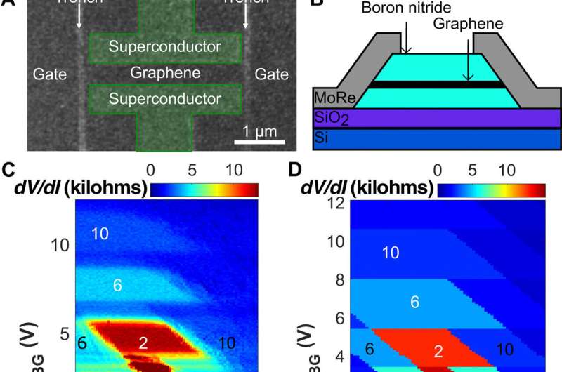
In the present work, Seredinski et al. examined a graphene Josephson junction with two graphene side gates to directly manipulate QH edge states. They tuned each gate to change the Landau level filling factor along the edges to observe a supercurrent, solely localized along one edge. The team built the samples from graphene encapsulated in hexagonal boron nitride (BN) to protect devices from contamination and to yield ballistic transport across micrometre scales. They etched the graphene-BN stack and then fabricated quasi-1-D contacts to the exposed region. They used molybdenum rhenium (MoRe), a type II superconductor and separated the 3-μm wide contacts by 500 nm to form the experimental setup. In the next step, they formed both the junction and side gates by etching narrow trenches on either side of the contacts, to efficiently control electron density along the edges of the junction—after applying voltage to the graphene regions. They did not overlap the etched trenches with the contacts and instead spaced them using a graphene strip, to prevent electrons from tunnelling directly from the superconductor to the edge.
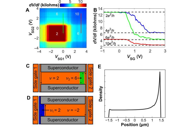
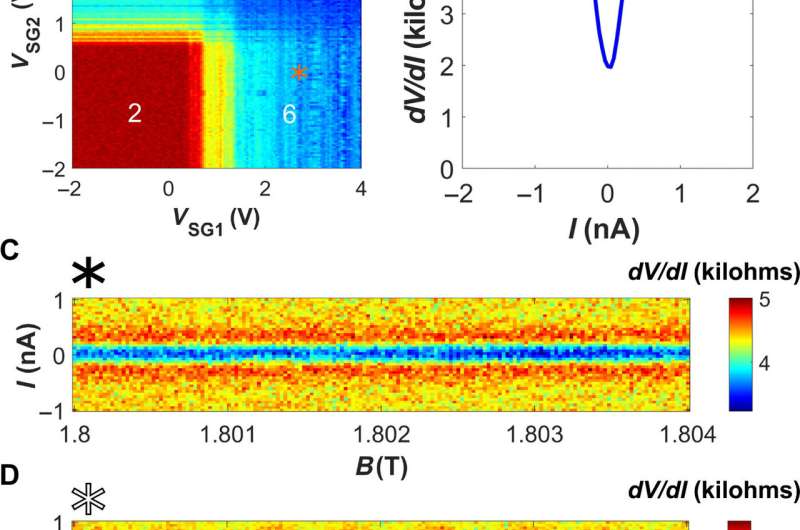
When Seredinksi et al. applied a magnetic field perpendicular to the sample, the junction entered the QH (quantum Hall) regime. By 1.8 Tesla, the QH effect was very well developed and observed using resistance maps reproduced by a simple electrostatic simulation in the work. The research team gained more insight to the function of the device by applying the side gates independently. They observed the influence of the side gates on the conductances to show negligible cross-talk between the left gate on the right edge, and vice-versa. The scientists tuned the gates to induce a QH state to create counter-propagating states within the device. The team observed the QH supercurrent and its interference patterns as a region of suppressed resistance flanked by peaks; characteristic of a small supercurrent. The team regulated features of the device to localize the supercurrent to either junction.

The supercurrent did not vary for small changes in the magnetic field. For example, when the team turned a side-gate on, the distance between the counter-propagating edge channels in the device facilitated the coupling of edge states to the superconductor—for the supercurrent to appear. When they applied both sides of the gates simultaneously, the dependence of the supercurrent on magnetic fields completely changed. The resulting map demonstrated a superconducting quantum interference device (SQUID)-like interference pattern. When Seredinski et al. explored the device as an interferometer for QH supercurrents, they changed the field to 1 T to observe a more robust supercharging signature. They obtained the pattern of resistance oscillations in the magnetic field, where the period of oscillations was independent of the gate voltage, while the phase of oscillations varied with the gate.

In an additional interference pattern, the research team observed the difference in the sample resistance between 0 and 10 nanoampere (nA) DC bias, to highlight the superconducting regions. They measured the map as a function of both side gates and observed the interference corresponding to supercurrents flowing along the side gate-1 (SG1) and side gate-2 (SG2). The two gates presented comparable efficiency. When the scientists increased the voltage of one gate, they decreased the voltage of the opposing gate to roughly maintain the same area of the SQUID (superconducting quantum interference device). These area changes were sufficient to evolve the phase of difference across the junction, although too small to create noticeable changes in the magnetic field periodicity.
![QH supercurrent interferometry. (A) dV/dI map measured at VSG1 = 2.34 V and VSG2 = 2.36 V as a function of VBG and B near 1 T. For a given gate voltage, the regions of suppressed resistance correspond to stronger supercurrent. The phase of the oscillations depends on the gate voltage, indicating that the interference area decreases with the gate voltage (positive dVBG/dB). This is explained by the inner edge states moving further inward as the electron density grows [schematic in (B)]. (B) Schematic of carrier density in the sample along the midline between the contacts. The blue line represents some baseline charge density; the green line shows a higher back gate voltage. (C) dV/dI map similar to (A) measured as a function of B and SG1 voltage for VBG = 3.8 V. The map shows an interference pattern with a slope opposite that in (A), indicating that the interference area increases with gate voltage as the electrons are pushed further toward the gate. (D) ΔR map displaying the difference between the resistance in the 0 and 10 nA DC bias conditions, measured at 1 T with VBG = 3.9 V. Both side-gate voltages are high enough to induce a supercurrent (VSG1,2 > 1 V), and the vertical and horizontal features correspond to the supercurrent induced by SG1 or SG2, respectively. At their intersections, additional diagonal features appear, indicating interference between the supercurrents on the two sides of the sample. The fringes have a slope ∼ −1, suggesting comparable efficiency of the two side gates. Credit: Science Advances, doi: 10.1126/sciadv.aaw8693. Quantum Hall-based superconducting interference device](https://scx1.b-cdn.net/csz/news/800a/2019/4-quantumhallb.jpg)
In this way, Andrew Seredinski and colleagues showed native graphene side gates to be remarkably efficient in controlling edge state propagation in the quantum Hall (QH) regime. They observed supercurrents induced by the side gates, to be carried by the QH edge states. These supercurrents flowed independently on each edge of the device and could be controlled independently by their corresponding gates. The experiment opens a promising new route to couple superconductors with QH edge states to induce non-Abelian excitations to form the basis of quantum computing architectures.
More information: Quantum Hall–based superconducting interference device. advances.sciencemag.org/content/5/9/eaaw8693 Andrew Seredinski et al. 13 September 2019, Science Advances.
Non-Abelian states of matter. www.ncbi.nlm.nih.gov/pubmed/20220836/ Stern A. et al. March 2010, Nature.
Non-Abelian anyons and topological quantum computation. journals.aps.org/rmp/abstract/ … 3/RevModPhys.80.1083 Chetan Nayak et al. 12 Sept 2008, Reviews of Modern Physics, APS Journals.
Supercurrent in the quantum Hall regime science.sciencemag.org/content/352/6288/966 Amet F. et al. 20 May 2016, Science.
Journal information: Science Advances , Nature , Science , Reviews of Modern Physics
© 2019 Science X Network


