August 22, 2019 feature
Ultrahigh thermal isolation across heterogeneously layered two-dimensional materials

Heterogeneous nanomaterials can now facilitate advanced electronics and photonics applications, but such progress is challenging for thermal applications due to the comparatively shorter wavelengths of heat carriers (known as phonons). In a new study, now published on Science Advances, Sam Vaziri and co-workers at Theiss Research and the departments of Electrical Engineering, Materials Science and Engineering at the National Institute of Standards and Technology (NIST), and the Precourt Institute of Energy at Stanford University, Stanford California, demonstrated unusually high thermal isolation across ultra-thin heterostructures.
They achieved this by layering atomically thin, two-dimensional (2-D) materials to form artificial stacks of monolayer graphene (Gr), molybdenum disulfide (MoS2)and tungsten diselenide (WSe2), with thermal resistance greater than silicon dioxide (SiO2). Alongside effective thermal conductivity lower than air at room temperature. Using Raman thermometry, the scientists simultaneously identified the thermal resistance between any 2-D monolayers in the stack to form thermal metamaterials as examples in the emerging field of phononics. Vaziri et al. propose applications of the metamaterials in ultrathin thermal insulation, thermal energy harvesting and to route heat within ultracompact geometries.
Advanced electronic and photonic devices such as high-electron mobility transistors, quantum cascade lasers and photonic bandgap crystals take advantage of the fermionic nature of charge carriers during voltage gating or confinement. Then they make use of long photon wavelengths during their interference. Nevertheless, thermal nanoengineering and the emerging field of phononics only offer a few examples, despite the existing demand for heat management applications. This discrepancy results from the short wavelengths of heat-carrying vibrations in solids, where the bosonic nature of phonons can also contribute to the challenge of actively controlling heat transport in solids where it cannot be voltage-gated like charge carriers.
![Optical and STEM characterization of vdW heterostructures. (A) Cross-section schematic of Gr/MoSe2/MoS2/WSe2 sandwich on SiO2/Si substrate, with the incident Raman laser. (B) Raman spectrum of such a heterostructure at the spot indicated by the red dot in the inset optical image. Raman signatures of all materials in the stack are obtained simultaneously. The graphene Raman spectrum is flattened to exclude the MoS2 photoluminescence (PL) effect. arb.u., arbitrary units. (C to F) STEM cross-sectional images of four-layer (C) and three-layer (D to F) heterostructures on SiO2. In (D), MoSe2 and WSe2 are approximately aligned along the 1H [100] zone axis, and in (E and F), the layers are misaligned by ~21° with respect to the 1H [100] zone axis. The monolayer graphene on top of each heterostructure is hard to discern due to the much lower atomic number of the carbon atoms. (G) PL spectra of monolayer MoS2, monolayer WSe2, and a Gr/MoS2/WSe2 heterostructure after annealing. The PL is strongly quenched in the heterostructure due to intimate interlayer coupling. Credit: Science Advances, doi: 10.1126/sciadv.aax1325 Ultrahigh thermal isolation across heterogeneously layered two-dimensional materials.](https://scx1.b-cdn.net/csz/news/800a/2019/1-ultrahighthe.jpg)
Physicists had previously attempted to manipulate the thermal properties of solids using non-laminate films and superlattices to reduce thermal conductivity below the constituent materials to ultimately achieve thermal manipulation via structural disorder and high interface density to introduce additional thermal resistance. They found unusually low thermal conductivity in nanoengineered silicon and germanium nanowires due to strong phonon-boundary scattering and achieved large thermal conductivities in isotopically pure materials such as diamond, graphene and boron arsenide via reduced phonon scattering.
Two dimensional (2-D) materials have thus enabled a new frontier with sub-nanometer thin, single monolayers to control device behaviors at atomic length scales. Existing examples include new tunneling field effect transistors and ultrathin photovoltaics with high efficiency. In the present work, Vaziri et al. used van der Waals (vdW) assembly of atomically thin 2-D layers to achieve unusually high thermal resistance across heterostructures. They showed a thermal resistance equivalent to 300 nm thick SiO2 across sub-2-nm-thin vdW heterostructures with clean, residue-free interfaces. By layering heterogeneous 2-D monolayers with diverse atomic densities and vibrational modes the research team demonstrated the potential to tailor thermal properties at the atomic scale; on the order of the phonon wavelength. The structural basis of the new phononic metamaterials with unusual properties is not commonly found in nature. The present work represents unique applications of 2-D materials and their weak vdW interactions for assembly to block or guide the flow of heat.

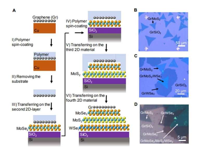
The research team obtained a cross-section of a four-layered heterostructure with graphene (Gr) on MoSe2 (molybdenum diselenide), MoS2 (molybdenum disulfide) and WSe2 (tungsten diselenide) on a SiO2/Si substrate. Using a Raman laser, they simultaneously probed the individual layers in the stack with single-layer accuracy. The research team separately grew the 2-D monolayer materials using chemical vapor deposition and transferred them to avoid polymer and other residues. To confirm the microstructural, thermal and electrical properties of the heterostructures, Vaziri et al. used extensive materials characterization techniques, including scanning transmission electron microscopy (STEM), photoluminescence (PL) spectroscopy, Kelvin probe microscopy (KLM) and scanning thermal microscopy (SThM) alongside Raman spectroscopy and thermometry. Using the techniques, they revealed the signature of every 2-D material monolayer in the stack and that of the Si substrate. Using multiple STEM images, the research team revealed atomically intimate vdW gaps without contaminants, allowing them to observe the total thickness of the heterostructures. They then confirmed interlayer coupling across large surface areas using PL spectroscopy.

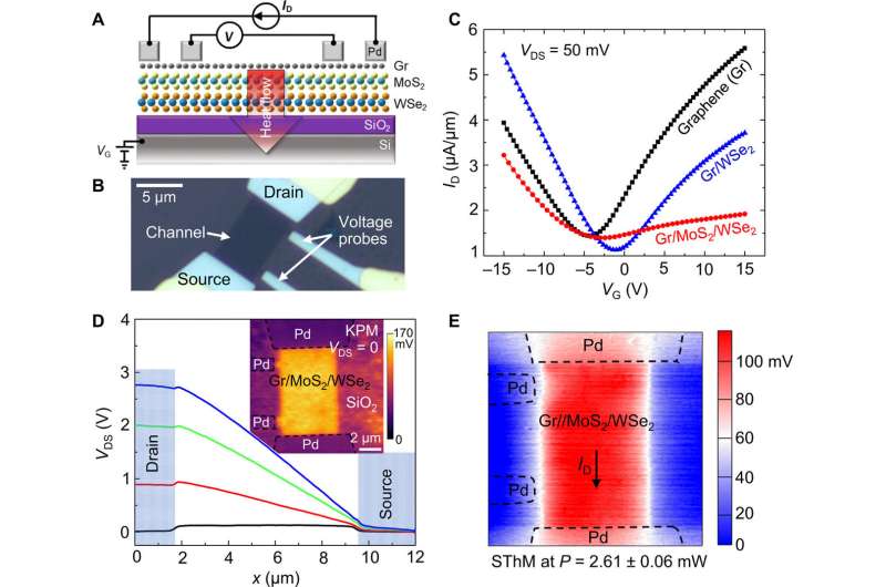
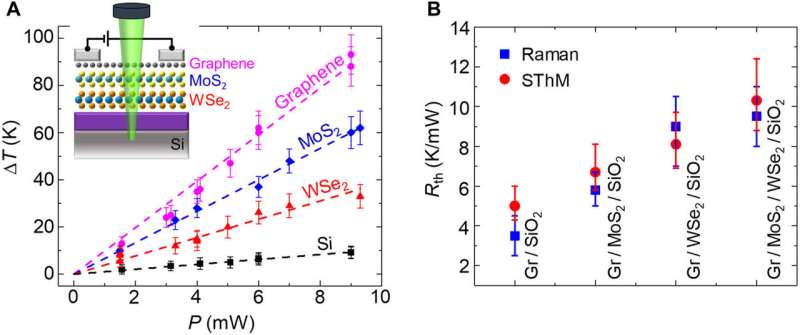
To measure heat flow perpendicular to the atomic planes of the heterostructure, Vaziri et al. patterned the stacks in the shape of four-probe electrical devices. They used electrical heating to accurately quantify the input power and confirmed the current conduction and heating on the top graphene layer to be orders of magnitude greater than for MoS2 and WSe2. To demonstrate the surface temperature uniformity of these devices they used KPM and SThM surface characterization methods and then quantified the temperature of each individual layer using Raman spectroscopy. As the graphene heat power (P) ramped up in the system, the temperature of each layer increased in a Gr/MoS2/WSe2 heterostructure setup. Due to uniform heating the researchers easily analyzed the thermal resistances from bottom to top. The excellent agreement between the two thermometry methods of Raman and SThM validated the values obtained in the setup.
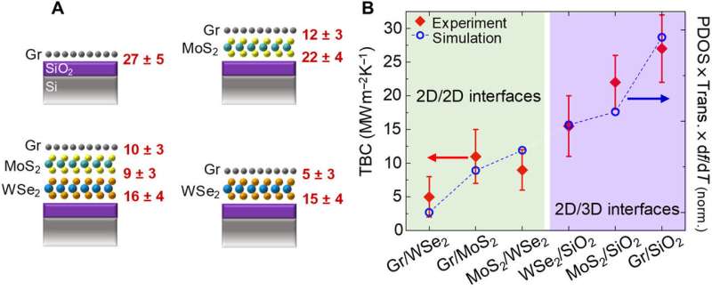
The scientists analyzed the thermal boundary resistance (TBR) between the layers responsible for the very large thermal resistance perpendicular to the heterostructures. The thermal boundary conductance (TBC) measurements in the study were a first for atomically intimate interfaces between 2-D/2-D monolayers and formed the first reported TBC between WSe2 and SiO2 monolayers. They showed that TBCs obtained for Gr/SiO2 and MOSe2/SiO2 interfaces agreed with previous studies, while TBC of the monolayer WSe2/SiO2 interface was comparatively lower, which was not unexpected due to the comparatively fewer flexural phonon modes available for transmission in the monolayer. According to the results, TBC for a 2-D/2-D interface was lower than the TBC with a 3-D SiO2 substrate. The lowest TBC recorded in the work belonged to Gr/WSe2 and the research team explained the observations using the Landauer formula. The research team obtained the phonon transmission at the interface using the acoustic mismatch model (AMM) as the ratio of mass density of the two materials. The researchers captured TBC trends using a simple model of heat flow across the interfaces developed in the study.

In this way, Sam Vaziri and co-workers gained knowledge to realize atomically tailored thermal interfaces and demonstrated their potential to engineer extremely thermally insulating metamaterials. The newly engineered metamaterials demonstrated properties unprecedented in nature. The heterostructures provide an example in the emerging fields of phononics to manipulate the thermal properties of solids at length scales comparable to phonon wavelengths. The 2-D layered materials offer promising, ultralight and compact heat shields to direct heat away from hotspots in electronics. The research team envision translating the metamaterials to improve the efficacy of thermoelectric energy harvesters and thermally active devices such as phase-change memories in the future.
More information: Sam Vaziri et al. Ultrahigh thermal isolation across heterogeneously layered two-dimensional materials, Science Advances (2019). DOI: 10.1126/sciadv.aax1325
Philip Ball. Computer engineering: Feeling the heat, Nature (2012). DOI: 10.1038/492174a
K. S. Novoselov et al. 2-D materials and van der Waals heterostructures, Science (2016). DOI: 10.1126/science.aac9439
Journal information: Science Advances , Nature , Science
© 2019 Science X Network


