August 30, 2019 feature
Quantum engineering atomically smooth single-crystalline silver films

Ultra-low-loss metal films with high-quality single crystals are in demand as the perfect surface for nanophotonics and quantum information processing applications. Silver is by far the most preferred material due to low-loss at optical and near infrared (near-IR) frequencies. In a recent study now published on Scientific Reports, Ilya A. Rodionov and an interdisciplinary research team in Germany and Russia reported a two-step approach for electronic beam evaporation of atomically smooth single crystalline metal films. They proposed a method to establish thermodynamic control of the film growth kinetics at the atomic level in order to deposit state-of-the-art metal films.
The researchers deposited 35 to 100 nm thick, single-crystalline silver films with sub-100 picometer (pm) surface roughness with theoretically limited optical losses to form ultrahigh-Q nanophotonic devices. They experimentally estimated the contribution of material purity, material grain boundaries, surface roughness and crystallinity to the optical properties of metal films. The team demonstrated a fundamental two-step approach for single-crystalline growth of silver, gold and aluminum films to open new possibilities in nanophotonics, biotechnology and superconductive quantum technologies. The research team intends to adopt the method to synthesize other extremely low-loss single-crystalline metal films.
Optoelectronic devices with plasmonic effects for near-field manipulation, amplification and sub-wavelength integration can open new frontiers in nanophotonics, quantum optics and in quantum information. Yet, the ohmic losses associated in metals are a considerable challenge to develop a variety of useful plasmonic devices. Materials scientists have devoted research efforts to clarify the influence of metal film properties to develop high performance material platforms. Single-crystalline platforms and nanoscale structural alterations can prevent this problem by eliminating material-induced scattering losses. While silver is one of the best known plasmonic metals at optical and near-IR frequencies, the metal can be challenging for single-crystalline film growth.

Previous reports on single-crystalline silver film growth methods relied on molecular beam epitaxy (MBE) or physical vapor deposition (PVD) with atomic smoothness and significantly lower optical losses. In the present study, Rodionov et al. used a two-step PVD growth approach previously developed by the same research team to obtain atomically smooth single-crystalline metal films using a high-vacuum electron-beam evaporator. The method facilitated high crystallinity and purity across an atomically smooth surface with unique optical properties and thermodynamic stability. The process is flexible, inexpensive and fast with a high deposition rate compared to the MBE technique. The team can replicate the method with a variety of metals including silver, gold and aluminum—widely used in quantum optics and quantum information.
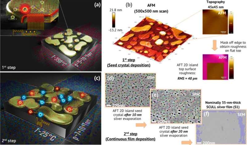
During the two-step deposition process for materials development, Rodionov et al. first grew a seed crystal containing strained two-dimensional silver islands (atomic features) with atomically flat top surfaces (AFT 2-D islands) on a substrate at 350 degrees C. According to the electronic growth model, silver islands are an electron gas confined to a 2-D quantum well (energy barriers that confine an electron). Then, the researchers cooled the substrate to 25 degrees C in the same vacuum cycle to prevent a dewetting effect. They evaporated the silver on the AFT 2-D seed to form a continuous single-crystal film to completion. Subsequently they annealed the silver film at higher temperatures (320-480 degrees C), which improved the crystalline structure and surface roughness of the resulting film. The scientists named their deposition process the SCULL—for "single-crystalline Continuous Ultra-Smooth Low-loss Low-cost"—thin-film production.

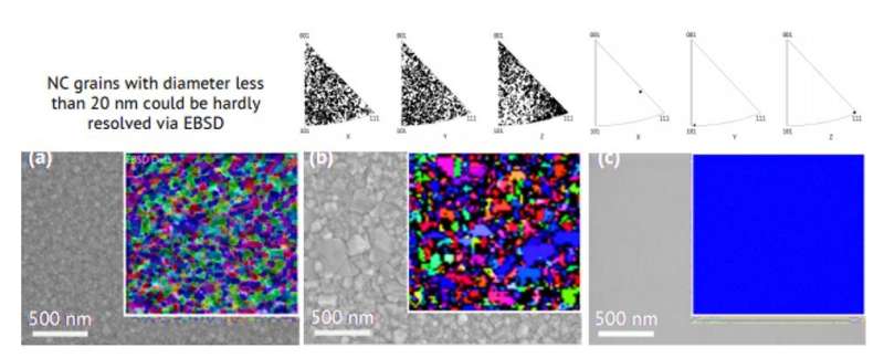
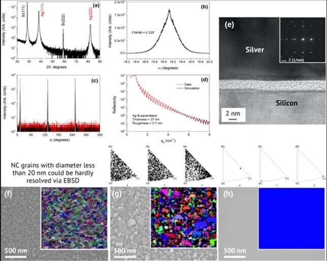
The research team developed materials using SCULL and compared the results for six representative films, which included three SCULL single crystalline films of varying thickness (35 nm, 70 nm and 100 nm) and three 100 nm thick polycrystalline films. The scientists used high-resolution wide-angle X-ray diffraction (XRD) to view the high quality of films with minimal levels of defect. Then using high-resolution transmission electron microscopy (HRTEM), the research team demonstrated the single-crystalline nature of the silver film. They used electron backscatter diffraction (EBSD) to analyze the domain structures and extract the average grain size of the single-crystalline and polycrystalline films.

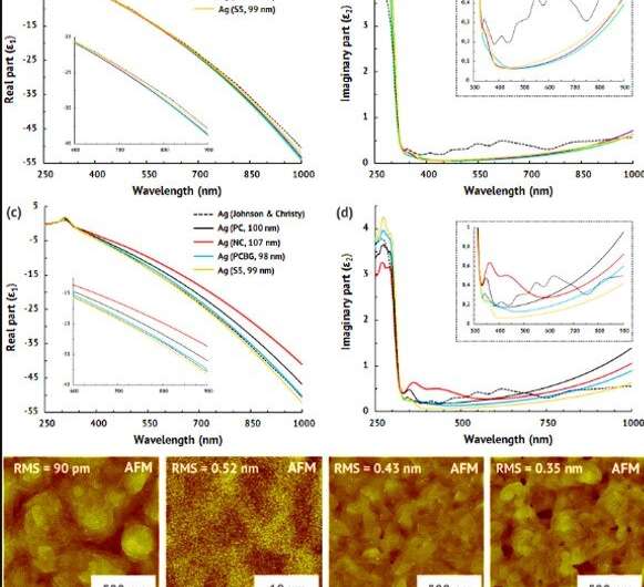
Rodionov et al. characterized the optical properties and surface topography of the single-crystalline films using atomic force microscopy. They then extensively demonstrated material purity and surface roughness to indicate a much purer silver film in the study. The SCULL silver films introduced in the work will have potential applications in the evolving field of quantum plasmonics and atomically smooth single-crystalline films that require low optical absorption and high conductivity. Rodionov et al. observed a theoretically predicted surface plasmon polariton propagation length for silver and exceptional performance of experimental plasmonic devices with the SCULL silver films.
In this way, Ilya A. Rodionov and co-workers developed a two-step approach for electronic beam evaporation to form continuous atomically smooth, single-crystalline metal films across a wider range of thickness from 35-100 nm. The researchers envision their proposed SCULL process will be used to deposit a variety of atomically smooth single crystalline thin films using an easy, top-down fabrication device in the future. The unique physical and optical properties of the resulting SCULL films can open new possibilities in diverse fields of technology.
More information: Ilya A. Rodionov et al. Quantum Engineering of Atomically Smooth Single-Crystalline Silver Films, Scientific Reports (2019). DOI: 10.1038/s41598-019-48508-3
P. Melentiev et al. Plasmonic nanolaser for intracavity spectroscopy and sensorics, Applied Physics Letters (2017). DOI: 10.1063/1.5003655
Harry A. Atwater et al. Plasmonics for improved photovoltaic devices, Nature Materials (2010). DOI: 10.1038/nmat2629
Journal information: Scientific Reports , Applied Physics Letters , Nature Materials
© 2019 Science X Network


