Ultra-clean fabrication platform produces nearly ideal 2-D transistors

Semiconductors, which are the basic building blocks of transistors, microprocessors, lasers, and LEDs, have driven advances in computing, memory, communications, and lighting technologies since the mid-20th century. Recently discovered two-dimensional materials, which feature many superlative properties, have the potential to advance these technologies, but creating 2-D devices with both good electrical contacts and stable performance has proved challenging.
Researchers at Columbia Engineering report that they have demonstrated a nearly ideal transistor made from a two-dimensional (2-D) material stack—with only a two-atom-thick semiconducting layer—by developing a completely clean and damage-free fabrication process. Their method shows vastly improved performance compared to 2-D semiconductors fabricated with a conventional process, and could provide a scalable platform for creating ultra-clean devices in the future. The study was published today in Nature Electronics.
"Making devices out of 2-D materials is a messy business," says James Teherani, assistant professor of electrical engineering. "Devices vary wildly from run to run and often degrade so fast that you see performance diminish while you're still measuring them."
Having grown tired of the inconsistent results, Teherani's team set out to develop a better way to make stable devices. "So," he explains, "we decided to separate the pristine device from the dirty fabrication processes that lead to variability."
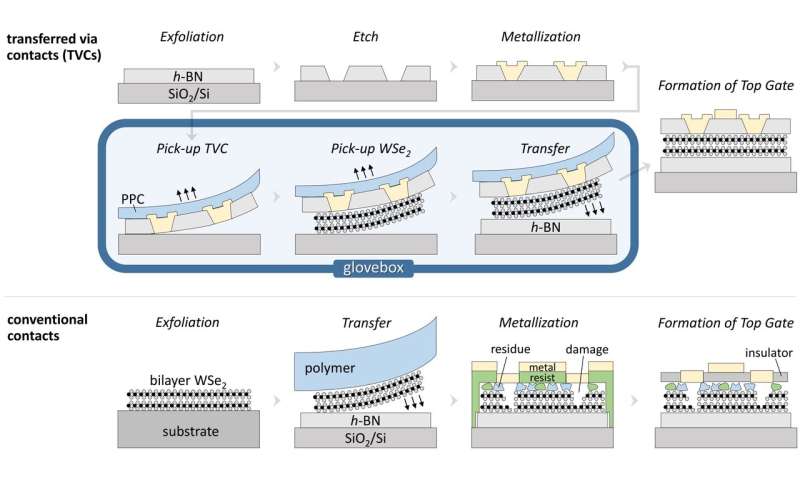
As shown in this new study, Teherani and his colleagues developed a two-step, ultra-clean nanofabrication process that separates the "messy" steps of fabrication—those that involve "dirty" metallization, chemicals, and polymers used to form electrical connections to the device—from the active semiconductor layer. Once they complete the messy fabrication, they could pick up the contacts and transfer them onto the clean active device layer, preserving the integrity of both layers.
"The thinness of these semiconductors is a blessing and a curse," says Teherani. "While the thinness allows them to be transparent and to be picked up and placed wherever you want them, the thinness also means there's nearly zero volume—the device is almost entirely surface. Because of this, any surface dirt or contamination will really degrade a device."
Currently, most devices are not encapsulated with a layer that protects the surface and contacts from contamination during fabrication. Teherani's team showed that their method can now not only protect the semiconductor layer so that they don't see performance degradation over time, but it can also yield high performance devices.
Teherani collaborated with Jim Hone, Wang Fong-Jen Professor of Mechanical Engineering, making use of the fabrication and analysis facilities of the Columbia Nano Initiative and the National Science Foundation-funded Materials Research Science and Engineering Center at Columbia. The team made the transferred contacts from metal embedded in insulating hexagonal boron nitride (h-BN) outside a glovebox and then dry-transferred the contact layer onto the 2-D semiconductor, which was kept pristine inside a nitrogen glovebox. This process prevents direct-metallization-induced damage while simultaneously providing encapsulation to protect the device.
-

The fabrication process for transferred contacts that yield nearly ideal transistors. Transferred contacts prevent contamination and damage to the 2D semiconductor that occur during fabrication of conventional contacts. Credit: Min Sup Choi/Columbia Engineering -

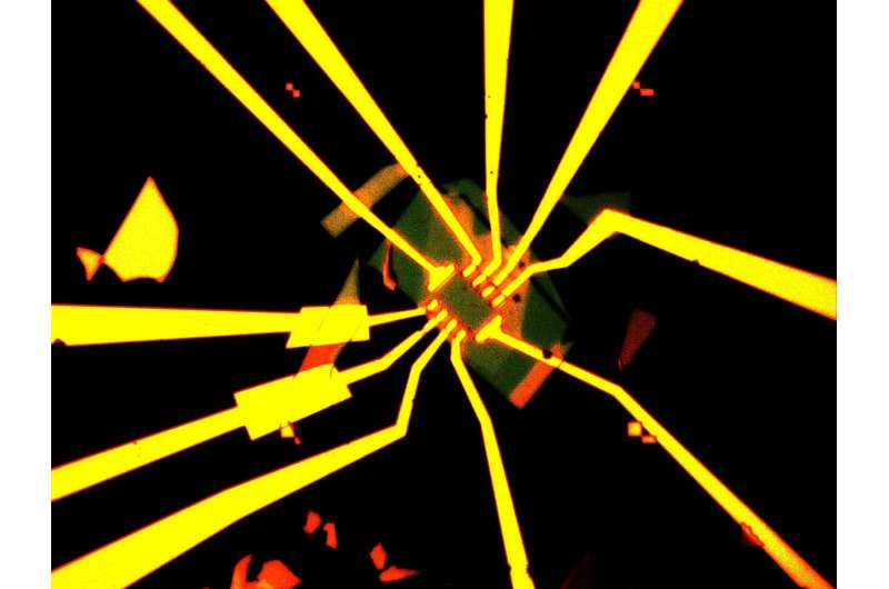
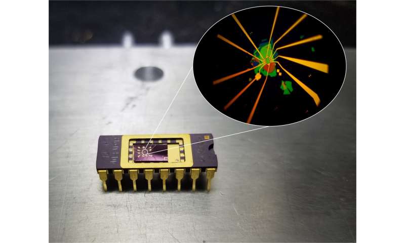
A Hall-bar device structure (see inset) is wire-bonded to a 16-pin chip-carrier. The chip-carrier allows for extensive electrical characterization of the device at both low temperatures and high magnetic fields. Credit: Min Sup Choi/Columbia Engineering
Now that the researchers have developed a stable, repeatable process, they are using the platform to make devices that can move out of the lab into real-world engineering problems.
"The development of high performance 2-D devices requires advances in the semiconductor materials from which they are made," Teherani adds. "More precise tools like ours will enable us to build more complex structures with potentially greater functionality and better performance."
The study is titled "Transferred via contacts as a platform for ideal two-dimensional transistors."
More information: Transferred via contacts as a platform for ideal two-dimensional transistors, Nature Electronics (2019). DOI: 10.1038/s41928-019-0245-y , dx.doi.org/10.1038/s41928-019-0245-y
Journal information: Nature Electronics


