May 29, 2019 feature
Atomic engineering with electric irradiation
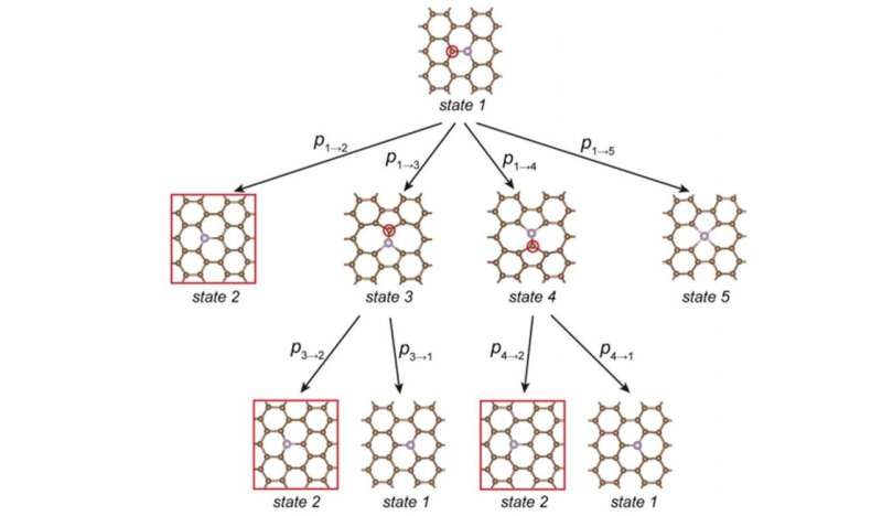
Atomic engineering can selectively induce specific dynamics on single atoms followed by combined steps to form large-scale assemblies thereafter. In a new study now published in Science Advances, Cong Su and an international, interdisciplinary team of scientists in the departments of Materials Science, Electronics, Physics, Nanoscience and Optoelectronic technology; first surveyed the single-step dynamics of graphene dopants. They then developed a theory to describe the probabilities of configurational outcomes based on the momentum of a primary knock-on atom post-collision in an experimental setup. Su et al. showed that the predicted branching ratio of configurational transformation agreed well with the single-atom experiments. The results suggest a way to bias single-atom dynamics to an outcome of interest and will pave the road to design and scale-up atomic engineering using electron irradiation.
Controlling the exact atomic structure of materials is an ultimate form of atomic engineering. Atomic manipulation and atom-by-atom assembly can create functional structures that are synthetically difficult to realize by exactly positioning the atomic dopants to modify the properties of carbon nanotubes and graphene. For example, in quantum informatics, nitrogen (N) or phosphorous (P) dopants can be incorporated due to their nonzero nuclear spin. To successfully conduct experimental atomic engineering, scientists must (1) understand how desirable local configurational change can be induced to increase the speed and the success rate of control, and (2) scale up the basic unit processes into feasible structural assemblies containing 1 to 1000 atoms to produce the desired functionality.
Researchers had previously used scanning tunneling microscopy to demonstrate good, stepwise control of single atoms to obtain physicochemical insights and technical advances. However, the scalability and throughput of the technique was severely limited by mechanical probe movements and therefore researchers introduced aberration-corrected scanning transmission electron microscopy (STEM) as a versatile tool to characterize the precise atomic structure of materials. Although still at early stages of development, the technique shows greater promise to control materials at the level of atoms. In two-dimensional (2-D) graphene, for instance, silicon dopants could be controlled stepwise to iterate basic steps that allowed the long-range movement with high throughput. Similar outcomes were also observed in a 3-D silicon crystal.
With STEM-based atomic engineering the scientists aim to use the beam of electrons and achieve a desired configurational change. Drawbacks of the method include imprecise understanding of relativistic electron-nucleus collisions, electronic excitation and relaxation, dynamic ion trajectories and added uncertainties.
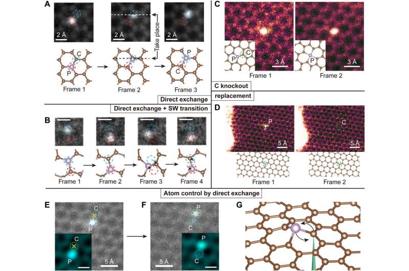
In the present work, Su et al. used STEM to drive and identify the motion of atoms in individual phosphorous (P) dopants within graphene. Followed by constructing a theoretical scheme to test relative probabilities of the dopants, compared to electron energy and momentum detection. They categorized the dynamics into four groups:
- Direct atomic exchange
- Stone-Wales transition which conserved the atoms (causing important chemical, electrical and mechanical property alterations due to atomic rearrangement.)
- Knockout of a carbon C neighbor, and
- Replacement of the dopant atom by carbon C, which did not conserve the local composition of the material.
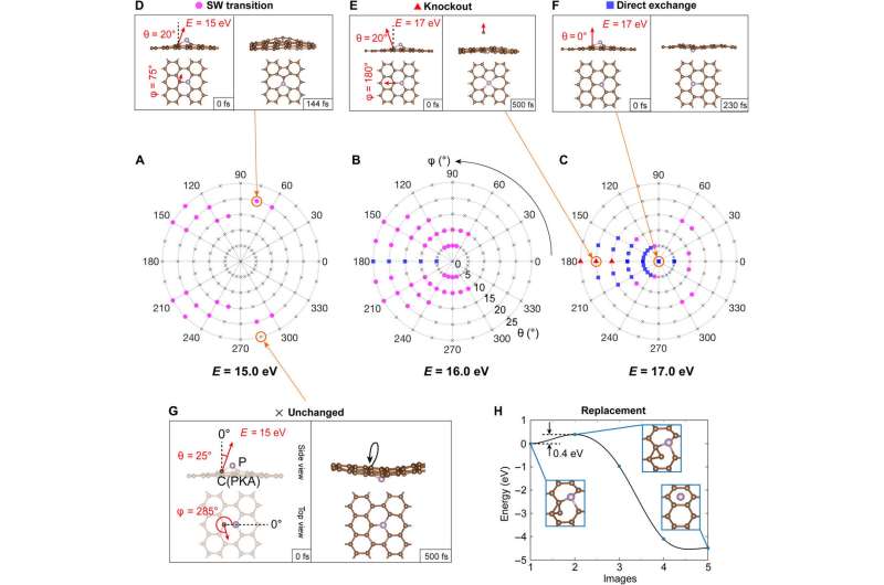
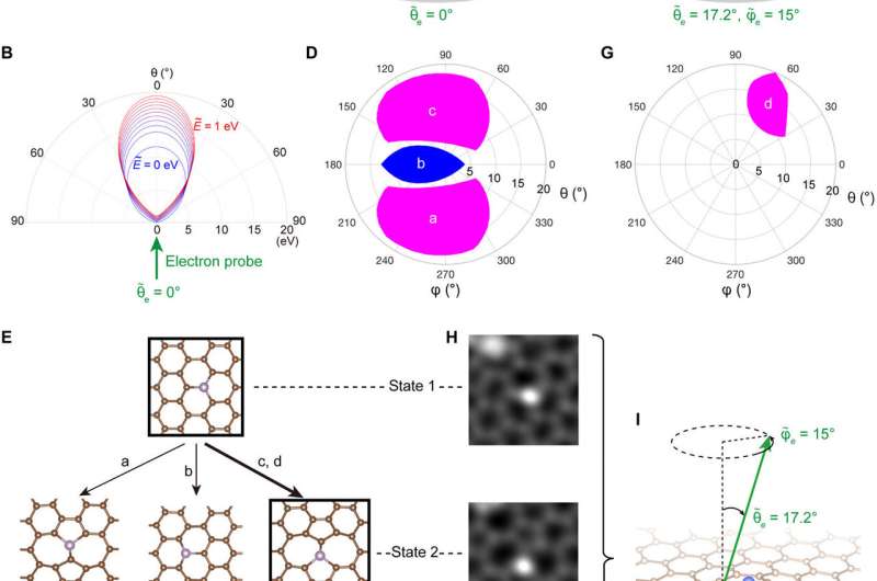
The scientists used a 60 eV electron energy beam and maximized the rates of direct exchange and SW transition during electron-atom collision. Su et al. used carbon as the primary knock-on atom (PKA) in the experiments and maintained a post-electron collisional energy of the PKA on the order of 10 eV. In the experiments, they did not aim the electron beam directly at the dopant itself, instead aiming at the carbon neighbor of the dopant.
Su et al. then developed a theoretical scheme in the study known as a "primary knock-on-space" (PKS) to estimate the relative scattering cross sections of diverse electron induced dynamics. The results could be varied due to sample or electron beam tilt to selectively activate the desired outcome. The scientists provided additional experimental verification of the calculations, opening new avenues for atomic engineering with focused electron irradiation.
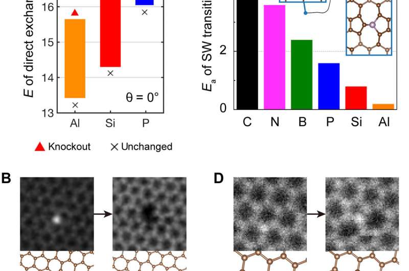
In practice, scientists aim to precisely control atoms and their electronic or nuclear states for applications in atomic clocks and atomic memory devices. The long-term vision of atomic engineering is to precisely position individual atoms in desired internal states to include nuclear spin, then image and control the atomic assemblies from 1 to 1000 atoms.
Su et al. realized several atomic dynamics in the present work, which they categorized as atom conserving dynamics (desired) or atom non-conserving dynamics (not desired). For atom conserving dynamics, they included (A) the direct exchange between phosphorous (dopant) and carbon. (B) SW transition with 90 degree rotation of a P-C bond, where the atom-conserving dynamics included a carbon knockout. Then for atom non-conserving dynamics, the scientists included (C) knockout of PKA using an electron beam and (D) replacement of the dopant atom.
To explain the atomic processes, the scientists performed extensive ab-initio molecular dynamics (abMD) simulations and climbing-image nudged elastic band (cNEB) calculations. They visualized the distribution of a variety of P dopant dynamics in correspondence to the initial post-collision kinetic energies of the PKA in graphene. The scientists induced a series of collisions with focused electrons via simulation, expecting to arrive experimentally at a predesigned configuration by controlling the electron beams for atomic configurational evolution, with relative ease.
In the study, the scientists started with an initial configurational state Iiniital that was precisely imaged in its desired trajectory of intermediate configurations to finally arrive at Ifinal; much like a Rubik's cube but with probabilities. Su et al. balanced the "risk" and "speed" when playing the game, as the atomic system could contain trap states (Itrap) to severely delay the arrival of atomic configuration to Ifinal or make its achievement improbable. The scientists also compared the probabilistic nature of the process to a game of soccer; where they used the computational prediction and the absolute transition rate to optimally engineer the total risk/speed-off in the experiment.
Since the process of predicting and comparing the scattering cross sections of dynamic processes is essential for atomic engineering, Su et al. developed a PKS (primary knock-on-space) formalism. Based on this, the scientists showed the momentum distribution of PKA had an ovoid profile after an electron collision, where the shape changed relative to the energy and direction of an incoming electron and due to pre-collisional momentum of the atom. The scientists propose the use of machine learning and artificial intelligence, to understand the unit and assembly processes in the future. In the present work, the scientists used a decision tree to predict the possible paths of evolution during atomic engineering, where the root node indicated the initial structure and child nodes inferred the next possible outcomes.
In this way, Su et al. revealed the physics of atomic engineering and used a computational/analytical framework as a foundation to develop further techniques to control single-atom dynamics in 3-D materials. The scientists aim to ultimately scale up multiple atoms starting from the single atom to assemble 1-1000 atoms in a desired configuration at high speed and efficacy.
More information: Cong Su, et al. Engineering single-atom dynamics with electron irradiation, Science Advances (2019). DOI: 10.1126/sciadv.aav2252
Jani Kotakoski, et al. Imaging atomic-level random walk of a point defect in graphene, Nature Communications (2014). DOI: 10.1038/ncomms4991
A. Ajoy, et al. Atomic-Scale Nuclear Spin Imaging Using Quantum-Assisted Sensors in Diamond, Physical Review X (2015). DOI: 10.1103/PhysRevX.5.011001
Journal information: Science Advances , Nature Communications , Physical Review X
© 2019 Science X Network


