New insights into semiconductors for spintronic applications from hard X-ray photoemission

"Spintronics" holds promise for new types of devices for information processing and data storage, with ones and zeros being stored in the spin state of electrons as well as their electric charge. Such devices could be faster and more energy efficient than current electronics.
Dilute magnetic semiconductors such as manganese-doped gallium arsenide are a promising material for spintronics, said Slavomir Nemsak, staff researcher at the Lawrence Berkeley National Laboratory and former postdoc in the UC Davis Department of Physics, working with Professor Charles Fadley and Adjunct Professor Claus Schneider. They have ferromagnetic properties but are not themselves metals. They are called "dilute" because the dopant makes up a small amount (a few percent) of the semiconductor material.
In a new study published Aug. 17 in Nature Communications, Nemsak, Fadley, Schneider and colleagues demonstrate the use of new techniques in X-ray spectroscopy to illuminate the internal structure of manganese-doped gallium arsenide.
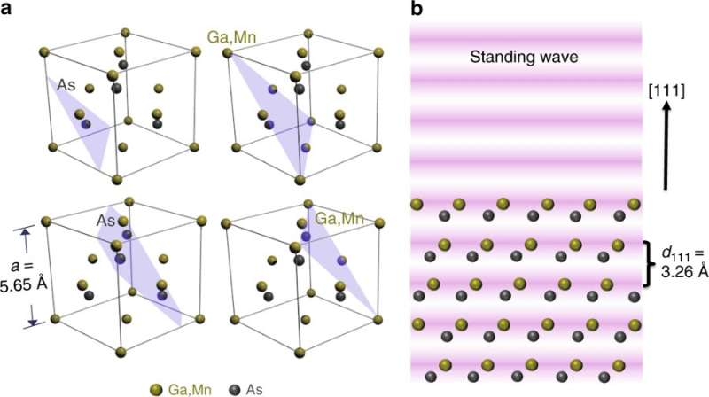
They used a technique called hard X-ray angle-resolved photoemission spectroscopy, or HARPES, combined with standing-wave excitation to obtain the unique and unprecedented look inside these promising new materials.
Standing-wave excitation allowed the researchers to enhance the electrical fields inside a material, creating peaks and troughs in each atomic layer. They could then determine which sites in a layer were occupied by gallium, arsenic or manganese atoms. The team combined this with the HARPES data, which gives information on how electrons determining the electric and optical properties behave in the material.
Connecting electronic states to elements
"We can use the standing wave to enhance the signal from gallium or arsenic layers, and we found that manganese was always present at the position of gallium atoms all the way from the bulk of material to its surface layers." Nemsak said. "We were also able to identify the changes in the electronics of the material caused by the presence of manganese dopant and connect the individual electronic states to their elemental origin."
This is the first time it has been possible to get this kind of information on structure and electronic properties from materials, Nemsak said. The technique should be applicable to any kind of material, including metals, semiconductors and insulators, and superconductors, he said.
The work with "hard" or high-energy X-rays was conducted using the Diamond Light Source at Didcot, U.K. This kind of study is currently possible with only a handful of facilities worldwide, including in the near future the Advanced Light Source at the Berkeley Lab.
More information: Slavomír Nemšák et al. Element- and momentum-resolved electronic structure of the dilute magnetic semiconductor manganese doped gallium arsenide, Nature Communications (2018). DOI: 10.1038/s41467-018-05823-z
Journal information: Nature Communications
Provided by UC Davis


