Splitting crystals for 2-D metallic conductivity

Sheets of electrons that are highly mobile in only two dimensions, known as 2-D electron gas, have unique properties that can be leveraged for faster and novel electronic devices. Researchers have been exploring 2-D electron gas, which was only discovered in 2004, to see how it can be used in superconductors, actuators and electronic memory devices, among others.
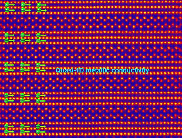
Researchers at Japan's Tohoku University, with an international team of colleagues, recently identified the atomic structure of a group of perovskite-related materials showing interesting 2-D conductive properties. The materials are made of strontium, niobium and oxygen atoms, with a layered structure derived from perovskite. These strontium niobate compounds show promise for developing advanced electronics due to their quasi-one-dimensional metallic conductivity.
Yuichi Ikuhara of Tohoku University's Advanced Institute for Materials Research with Johannes Georg Bednorz of Zürich Research Laboratory and colleagues used atom-resolved scanning transmission electron microscopy combined with theoretical calculations to learn how adding oxygen atoms to strontium niobates affects their conductivity. Four different materials formed depending on the concentration of oxygen atoms.
The researchers found that three of the materials were conductors of electricity while the fourth was an insulator. At the atomic scale, they discovered the materials were formed of alternating chain-like and zigzag slabs. Depending on the concentration of oxygen atoms, the chain-like slabs were two, three, or four layers thick, sometimes varying within the same material. The zigzag slabs were insulating layers in all the materials, while the chain-like slabs were conducting layers in three of the four materials.
The team determined that local electrical conductivity within the material directly depended on the shapes of the niobate octahedra in the layers. When positive ions of niobium were displaced toward the centers of the niobate octahedra, a local conducting nature was induced.
2-D conducting layers are commonly formed by creating an interface between two insulators. It should now be possible to achieve the same goal by segmenting 3-D conducting materials into stacks of 2-D conducting layers separated by insulating layers, the researchers say in their study published in the journal ACS Nano. This could lead to applications in the development of 2-D electrical conducting materials and devices.
More information: Chunlin Chen et al, Atomic-Scale Origin of the Quasi-One-Dimensional Metallic Conductivity in Strontium Niobates with Perovskite-Related Layered Structures, ACS Nano (2017). DOI: 10.1021/acsnano.7b06619
Journal information: ACS Nano
Provided by Tohoku University


