January 4, 2018 report
Creating 2-D dichalcogenide structures using chemical vapor deposition

A team of researchers from the University of South Florida and Florida State University has developed a one-pot synthesis technique for creating 2-D multi-junction heterostructures. In their paper published in the journal Nature, the team describes their technique and why they believe it will be useful for building future high-speed electronics and optoelectronic devices. Weijie Zhao and Qihua Xiong with Nanyang Technological University in Singapore offer a News and Views piece in the same journal issue outlining the work done by the team in Florida.
As scientists continue to study the possible benefits and uses of 2-D semiconductors, they have found that they must also study heterostructures—tiny structures that serve as interfaces between 2-D semiconductors and other 2-D semiconductors. Prior research has narrowed the options down to vertical or lateral heterostructures. Current one-step methods for creating lateral heterostructures lack flexibility—they can only produce one type of heterostructure—and two-step (or multi-step) methods involve making many changes to precursors and reaction chambers, making them difficult to carry out. In this new effort, the team in Florida has found a way to create multiple types of heterostructures using a one-pot technique that allows several steps to be carried out in a single reaction chamber.
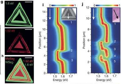
The new approach, as Zhao and Xiong note, is based on chemical vapor deposition—they expose a substrate to a gaseous precursor, which deposits heterostructures as part of a reaction process. The new technique employs the use of a carrier gas to bring transition-metal dichalcogenides, generically written as MX2, into contact with the substrate—in this case, 2-D MoX2 and WX2. Furthermore, they found that the heterostructures that were grown due to the reactions in the chamber could be switched by changing the carrier gas. This approach produced multiple types of heterostructures in a single reaction chamber. The group looked at their results with high-resolution transmission electron microscopy to make sure the heterostructures grew as expected, and report that they did. They also conducted spectroscopic analysis of their work to show that the junctions were made in a way that was reproducible. They then created primitive electrical devices to show that they worked as intended.
Zhao and Xiong note that because their technique is relatively simple, it appears their approach has the potential to be useful in manufacturing desired devices including flexible electronics.
More information: Prasana K. Sahoo et al. One-pot growth of two-dimensional lateral heterostructures via sequential edge-epitaxy, Nature (2018). DOI: 10.1038/nature25155
Abstract
Growing lateral heterostructures of two-dimensional (2D) dichalcogenide structures via chemical vapour deposition opens up new opportunities for building 2D electronic and optoelectronic devices. But it is challenging to make multiple spatially defined lateral heterostructures. This paper reports a straightforward one-pot approach to growing 2D multi-junction heterostructures by switching the gas environment in the presence of water vapour flowing over the solid sources of both MoX2 and WX2 powders placed in the same boat. The gas environment regulates the precursor species in the vapour phase via precursor volatilization and water-induced oxidation and can thus control their preferential deposition. Humberto Gutiérrez and colleagues use this technique to create multiple heterostructures of MoX2 and WX2 in one reactor and to make alloyed sulfide/selenide heterostructures.
Journal information: Nature
© 2018 Phys.org


