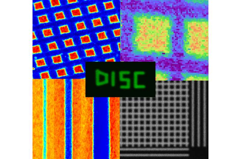
Exploiting reversible solubility allows for direct, optical patterning of unprecedentedly small features.

To build better solar cells, scientists need to design materials from the bottom up, placing chains of molecules just where they are needed. Scientists devised a new way to grow neatly arranged, densely packed bundles of molecular chains, specifically semiconducting polymer chains. The chains folded on themselves to make bundles that stretched from the growth plate to the film's surface. The bundles were packed side-by-side with neighboring bundles. This bottom-up approach, starting with the building blocks and creating the larger structure, was used to make large-area films with tiny patterns. The films have controlled architecture, uniform assembly and excellent stability.
The thin films of semiconducting polymers have a unique structure and are highly stable. The films could increase the efficiency and lifetime of organic light-emitting devices and solar cells.
Traditional methods using "top-down" solution-based processing typically only allow modest control over the molecular organization and chain alignment of semiconducting polymers. Now a team led by scientists at Louisiana State University have developed a "bottom-up" approach using surface-initiated growth of a semiconducting polymer called polythiophene to prepare thin films. Polythiophene is a promising organic electronic material. Extensive structural studies of the thin films using x-ray and neutron scattering revealed detailed information on the unique molecular organization and the bulk morphology of the films. The studies also further our fundamental understanding of the polymerization. Remarkably, the polymer chains formed densely packed lateral crystalline domains spanning about 3 nanometers, with predominant in-plane alignment of the folded polymer chains within each domain. Achieving such a complex intermediate-scale organization is virtually impossible with traditional methods relying on solution processing of pre-synthesized polymers. This unique morphology would be particularly suited for applications requiring efficient charge transport across the films, such as in photovoltaic and light-emitting devices. In general, surface-initiated polymerization is not limited to polythiophene but can also be expanded for other classes of semiconducting polymers and copolymers.
More information: Sang Gil Youm et al. Polythiophene Thin Films by Surface-Initiated Polymerization: Mechanistic and Structural Studies, Chemistry of Materials (2016). DOI: 10.1021/acs.chemmater.6b01957
Journal information: Chemistry of Materials
Provided by US Department of Energy


