X-ray imaging and computer modeling help map electric properties of nanomaterials

With the tap of your finger, your tablet comes to life – thanks to tiny force sensors and accelerometers that contain piezoelectric materials.
These materials generate electricity whenever mechanical pressure is applied to them, and they've helped shape how we use and interact with technology today. Piezoelectric devices can be found everywhere, from consumer electronics like wearable fitness trackers and smart clothing, to medical devices and motors.
Now researchers at the U.S. Department of Energy's (DOE) Argonne National Laboratory have developed a new approach for studying piezoelectric materials by using ultrafast 3-D X-ray imaging and computer modeling. Their integrated approach, reported in Nano Letters, can help us better understand material behavior and engineer more powerful and energy-efficient technologies.
"Our approach reveals a wealth of information about the underlying mechanisms that regulate the transfer of energy in such materials, as well as how stable these materials are under extreme conditions," said Argonne computational scientist and co-author Subramanian Sankaranarayanan.
"Using experimental data, we make informed models which in turn make predictions at space and time scales that experiments cannot reach," said Mathew Cherukara, the lead author of the study.
The researchers applied their new approach to the study of zinc oxide, a material that can generate electricity when twisted, bent or deformed in other ways. With its desirable piezoelectric and semiconducting properties, zinc oxide has emerged as a promising material for generating electricity in small-scale devices.
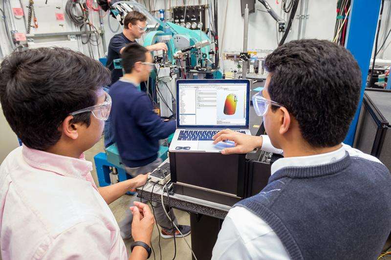
In their experimental approach, known as ultrafast X-ray coherent imaging, researchers took a nanocrystal of zinc oxide and exposed it to intense, short X-ray and optical laser pulses at Argonne's Advanced Photon Source, a DOE Office of Science User Facility. The ultrafast laser pulses excited the crystal, and the X-ray pulses imaged the crystal structure as it changed over time. This enabled researchers to capture very small changes in the material at a high resolution in both time and space.
"Unlike an optical microscope, which enables you to see an object but doesn't allow you to see what's happening inside of it, X-ray coherent diffractive imaging lets us see inside materials as they're bending, twisting and deforming, in full 3-D," said Argonne physicist and co-author Ross Harder. This is the first time such a time-resolved study has been performed at a synchrotron source.
Researchers identified the deformation modes – meaning new ways in which the material could bend, twist, rotate, etc. – from this experimental approach, and used this insight to build a model that would describe the behavior of the nanocrystal.
"By integrating theory and modeling with experiments, we're providing a more complete picture of the material behavior," said Argonne postdoctoral researcher and lead theory author Kiran Sasikumar. "Modeling provides additional insight into the problem – insights that experiments alone cannot probe."
With this model, researchers discovered additional twisting modes that can generate 50 percent more electricity than the bending modes of the crystal.
"Now we can use this information to create devices that exploit these twisting modes," Cherukara said. "This additional insight generated from the theory demonstrates how experimentation and theory together can enable us to make more accurate and useful predictions."
Combining modeling and experimental approaches can also help researchers explore various other material systems and processes, such as corrosion and heat management across thermal devices. Such work will also be advanced with the upgrade of the Advanced Photon Source, which will increase the flux of the facility's high-energy coherent X-ray beams by one hundred fifty-fold, the researchers said.
"With this upgrade, we'll be able to apply coherent imaging techniques to a wider class of materials, with less data acquisition time and even higher spatial resolution," said Argonne physicist and co-author Haidan Wen.
The study, titled "Ultrafast Three-Dimensional X-ray Imaging of Deformation Modes in ZnO Nanocrystals" was published in Nano Letters.
More information: Mathew J. Cherukara et al. Ultrafast Three-Dimensional X-ray Imaging of Deformation Modes in ZnO Nanocrystals, Nano Letters (2017). DOI: 10.1021/acs.nanolett.6b04652
Journal information: Nano Letters
Provided by Argonne National Laboratory


