Scalable 100 percent yield production of conductive graphene inks

Conductive inks are useful for a range of applications, including printed and flexible electronics such as radio frequency identification (RFID) antennas, transistors or photovoltaic cells. The advent of the internet of things is predicted to lead to new connectivity within everyday objects, including in food packaging. There is a clear need for cheap and efficient production of electronic devices using stable, conductive and non-toxic components.
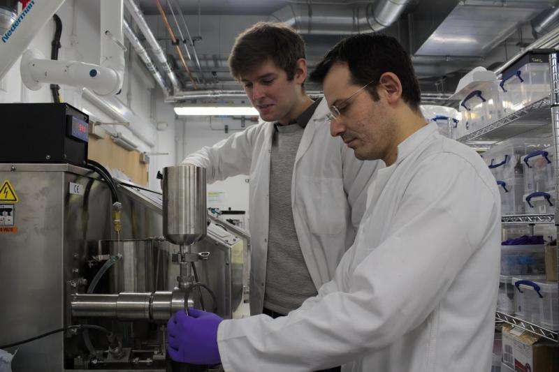
A new method for producing high quality, water-based conductive graphene inks with high concentrations has been developed by researchers from the Graphene Flagship working at the Cambridge Graphene Centre at the University of Cambridge, UK. The novel method uses ultrahigh shear forces in a microfluidisation process to exfoliate graphene flakes from graphite. The process converts 100% of the starting graphite material into usable flakes for conductive inks, avoiding the need for centrifugation and reducing the time taken to produce a usable ink. The research is published in ACS Nano.
The inks produced by the microfluidisation process have high concentrations of up to 100 g of graphene flakes per litre and can be optimised for screen printing. These inks can also be used to create novel composites, coatings and energy storage devices. This method can easily be applied to other layered materials, such as hexagonal boron nitride or transition metal dichalcogenides, to provide a family of printable circuit components – conductor, insulators and semiconductors – with which to build printed electronics with different functionalities. These inks are ideal for applications where low-cost is important.
With the 100% yield of the microfluidisation method, it is now possible to produce high quality graphene inks in sufficient quantities for commercial products. Inks produced using this method have already been commercialised via a University of Cambridge spin out company, Cambridge Graphene, which was recently acquired by engineering solutions company Versarien. The inks are also supplied to Novalia, an innovative print company based in Cambridge, for use in their interactive touch-based printed electronic demos.

Dr. Panagiotis Karagiannidis, a researcher at the Cambridge Graphene Centre, is lead author of the work. "The motivation was the need for layers with low sheet resistance to be produced by screen printing using inks with high concentration. In the microfluidisation process, all of the starting mixture experiences the same uniform intensive shear levels, converting it into a usable ink with high concentration. There is no wastage of material or time consuming post-processing."
Prof. Andrea Ferrari is Director of the Cambridge Graphene Centre, Science and Technology Officer of the Graphene Flagship, and Chair of the Flagship Management Panel. He stated "This is an important conceptual advance, and will significantly help the innovation and industrialization goals of the Graphene Flagship. The fact that the process is already licensed and commercialized indicates how it is feasible to cut the time from lab to market even during the lifetime of the Flagship."
Chris Jones of Novalia said "For viable marketable applications, the materials need to be cost effective, easy to handle and show consistent performance. We ran these inks on ordinary industrial screen printing equipment without modification and achieved consistent results, printing hundreds of interactive demonstrators for Mobile World Congress. This is a very exciting point - a critical juncture between the laboratory and the public."
Mar García-Hernandez of the Spanish National Research Council (CSIC) is the leader of the Graphene Flagship Work Package Enabling Materials, which is focused on development of scalable synthesis methods for graphene and other layered materials. "Microfluidisation is a huge leap ahead towards applications of affordable and environmentally friendly graphene inks in organic photovoltaics, RFID antennas, electrically conductive coatings or nanocomposites. The method is certainly well suited for the synthesis of a variety of other layered material inks, which will enlarge the scope of applications of layered materials in real world devices."
More information: Panagiotis G. Karagiannidis et al. Microfluidization of Graphite and Formulation of Graphene-Based Conductive Inks, ACS Nano (2017). DOI: 10.1021/acsnano.6b07735
Journal information: ACS Nano
Provided by Graphene Flagship


