Researchers use holography to improve nanophotonic circuits

Nanophotonic circuits, tiny chips which filter and steer light, suffer from small random variations which degrade the transmission of light. Researchers have now found a way to compensate those variations, which may lead to energy savings in datacenters and computer equipment. The researchers from Utrecht University (Debye Institute), University of Twente (MESA+ Institute for Nanotechnology) and Thales Research & Technology France published their results in the leading optical journal Optics Express on 21 February.
Optical communication is adopted worldwide: basically every high-speed internet connection nowadays is provided by optical fibers. Today, an active area of development is the use of optical communication on the scale of a single chip, to reduce power consumption in computers and data centers. One of the promising ways to steer the light propagation on such a chip is to use coupled photonic crystal nanoresonators, where light is transmitted between resonators that are tuned to the exact same resonance frequency. These frequencies are determined by the shape and structure of each resonator. However, even the best nanofabrication possible today, in which the holes are placed with a precision of ten times the diameter of an atom, small random variations induce changes in the resonance frequencies, which degrade the transmission of light.
Digital holography techniques
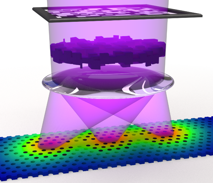
The researchers have now proposed and experimentally demonstrated an optical method to control photonic crystal nanoresonators. They employ digital holography techniques to focus several spots of laser light at definite positions. The laser light locally heats the nanophotonic chip and undoes the random variations. Moreover, this method enables the researchers to program photonic circuits by switching them into and out of resonance. The results, published in the open access journal Optics Express, will contribute to the ongoing development of low-power high-performance communication and computer equipment.
More information: Sergei Sokolov et al. Tuning out disorder-induced localization in nanophotonic cavity arrays, Optics Express (2017). DOI: 10.1364/OE.25.004598
Journal information: Optics Express
Provided by Utrecht University Faculty of Science


