Materials study probes 'field-assisted' processing for high-tech ceramic components

A new project will study the fundamental mechanisms behind a method that uses electrical fields to enhance ceramics-sintering processing to manufacture components for a range of military and commercial applications.
The components are expensive to manufacture because they are traditionally created from a powder that is sintered – or fused together – at around 1,500 degrees Centigrade for several hours.
Now, researchers are working to better understand a new technique that could reduce manufacturing costs while dramatically speeding the process. The team will study field-assisted sintering technology (FAST), where applying an electric field enhances sintering. A form of FAST, called flash sintering, takes only seconds and reduces the processing temperature by 50 percent or less, to roughly 800 degrees Centigrade.
"Our scope is to understand why within a matter of seconds and at such a low temperature you can facilitate sintering, which conventionally needs a much longer time at higher temperature," said Haiyan Wang, the Basil S. Turner Professor of Engineering in Purdue University's School of Materials Engineering. "Despite successful demonstrations of flash sintering, it remains poorly understood at the atomic scale."
Understanding the mechanisms behind the FAST process could speed commercial development of bulk ceramic sintering processing for a range of applications. The same mechanisms also apply to other applications beyond flash sintering such as research into rechargeable lithium-ion batteries and fuel cells, where charged ions play a critical role in the overall functionalities.
The project is funded with a $3 million four-year grant from the U.S. Office of Naval Research and is led by Wang, working with two co-principal investigators at Purdue and collaborators at the University of California, Davis; Rutgers University; Colorado State University and the Naval Research Laboratory.
"We need to develop a comprehensive scientific understanding along with predictive modeling tools and a set of rules and guidelines related to electrically assisted materials manufacturing of ceramics," Wang said.
Key members of the team are: Edwin García and Xinghang Zhang, both professors in Purdue's School of Materials Engineering; Amiya Mukherjee, a distinguished professor of materials science and engineering at UC Davis; Thomas Tsakalakos, a distinguished professor of materials science and engineering at Rutgers; Troy Holland, an assistant professor of mechanical engineering at Colorado State University; and Naval Research Laboratory physicists C. Stephen Hellberg, Noam Bernstein and Steven Erwin. The project also will involve several doctoral students and postdoctoral research associates.

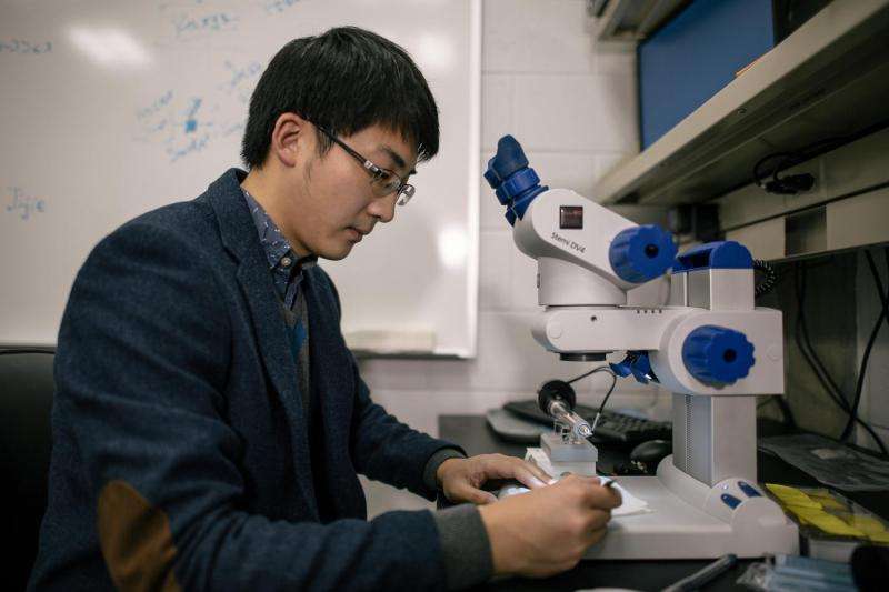
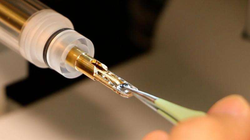
Critical to the research at Purdue are laboratory tools called in-situ transmission electron microscopy and in-situ scanning electron microscopy. The techniques allow researchers to "see" what's going on in the crystal structure of the ceramic material at the atomic scale while it is being sintered. The crystal structure is made up of faceted "grains" 100 nanometers in diameter, which is too small to be seen with conventional light microscopes. Researchers will take real-time video of the process.
"Macroscopic descriptions of flash-sintering-related phenomena exist, but micro- or nano- scale understanding is still lacking," Wang said.
Although ceramics are electrically insulating, they can conduct ions, or charged atoms. This flow of ions is sufficient to sinter the material at far lower temperatures than ordinarily required. The ions "hop" from sites on a ceramic's crystal lattice structure. If oxygen atoms are missing from some sites in the crystal lattice, a positive charge is created at these sites, attracting the negatively charged ions.
The researchers are studying the phenomenon in a ceramic called yttria-stabilized zirconia and two other ceramics that have a large number of "oxygen vacancies" in their crystal structure.

"The energy required for this hopping is quite high, but an interesting twist is that this type of ceramic has unique oxygen hopping channels," Wang said.
The research team will pursue three objectives: understanding the interactions between the electric field and matter under processing conditions; providing theories and software for science and engineering; and developing rules and guidelines for materials engineers to use in manufacturing settings.
In addition, findings could be mined and used to generate predictive models with "machine learning" methods, which could help engineers and technologists choose the correct materials to use for a given task. The research also could shed light on a phenomenon called electromigration, which can affect the performance of electronic devices.
Provided by Purdue University


