Scientists discover a way to control the electrical current in a new ultra-thin layered material

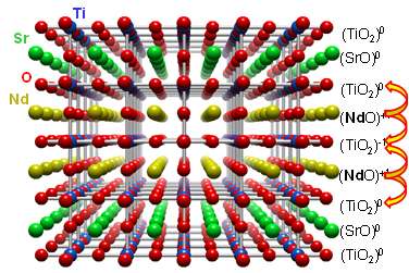
By modifying the composition of ultra-thin layers of dissimilar metal oxides that do not normally conduct electricity, scientists demonstrated how to generate and control an electrical current at the junction where the layers meet. The team made significant advances in one method used to characterize these materials. This work represents a major advance in the field of thin-film engineering. It shows that the properties of materials can be controlled at the level of the individual particles that constitute the materials. Some of the materials in the investigated structures are only one atomic layer thick, and yet their properties can be controlled.
The materials required for the next generation of electronic devices, including cell phones and laptop computers, must be able to operate on a size scale much smaller and more energy efficient than is possible with today's materials. This work represents a significant step in that direction.
Ultra-thin, alternating layers of neodymium titanium oxide (NdTiO3) and strontium titanium oxide (SrTiO3) were deposited by generating beams of the constituent elements (Nd, Ti, Sr, and O) in an ultra-clean vacuum environment, and aiming these beams at a small wafer of a crystalline oxide. This oxide wafer functioned as the foundation for the layered thin-film material, allowing the atoms to crystallize into the desired structure. The sequencing of the elemental beams allowed the layered structure to be precisely controlled, down to the level of single atomic layers.
They characterized the composite material using a number of materials analysis methods. However, accurate interpretation of some of these data, specifically x-ray photoelectron spectra (XPS), required advanced theoretical modeling. This modeling yielded definitive insights into how changes in composition brought about by both environmental factors and film growth processing conditions were effecting the electronic environment surrounding the titanium atoms. The scientists then measured and interpreted the electrical properties of the multi-layer structure in light of accurate knowledge of the valence and dielectric environment of titanium atoms in the different layers.
The result is unique and a powerful insight into how to make a two-dimensional electron gas in which the carrier concentration can be precisely controlled and engineered to reach a sufficiently high value to enable a new generation of ultra-small transistors to be envisaged.
The immediate next step is to determine the complex atomic structure of the interface between NdTiO3 and SrTiO3 as this structure determines the density of electrons that can be achieved in the two-dimensional electron gas within the SrTiO3.
More information: Peng Xu et al. Predictive Control over Charge Density in the Two-Dimensional Electron Gas at the Polar-NonpolarInterface, Physical Review Letters (2016). DOI: 10.1103/PhysRevLett.117.106803
Journal information: Physical Review Letters
Provided by Pacific Northwest National Laboratory


