September 21, 2016 report
More precise measurements of phosphorene suggest it has advantages over other 2-D materials

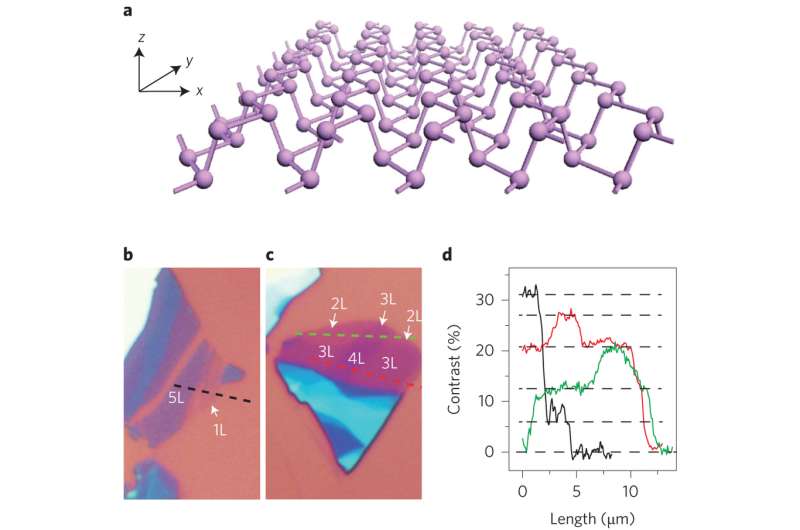
(Phys.org)—A large team of researchers from China, the U.S. and Japan has developed a more precise means for measuring the various band gaps in layered phosphorene, and in so doing, have found that it possesses advantages over other 2-D materials. In their paper published in the journal Nature Nanotechnology, the group describes their technique and what they observed during their measurements.
Scientists have been studying phosphorene (single layered black phosphorus) for some time because they believe it might be useful for creating new or better types of 2-D optoelectronic devices, similar in some respects to research efforts looking into graphene. Though it was first discovered in 1669, it was not actually isolated until 2014. Since that time, researchers have attempted to study the band gaps (the energy differences between the tops of the valence bands and the bottom of the conduction bands) that exist under various layering conditions because each may represent a unique opportunity for using the material. Prior efforts to find the band gaps relied on fluorescence spectroscopy, but that technique has not offered the accuracy needed for building devices. In this new effort, the researchers took a new approach called optical absorption spectroscopy, which works by measuring absorption of radiation as it interacts with a sample. By conducting multiple experiments, the researchers found that the electronic structure of the material varied significantly when looking at materials created from a range of layers, which, they noted, was consistent with prior theories.
In using the new technique, the researchers found that different band gaps aligned well with different applications. 1.15eV, for example, would match well with a silicon band gap and 0.83 eV could be used in optoelectronics because of its similarity to a telecom photon wavelength. Also, they noted that the 0.35 eV band gap could prove useful in creating infrared devices. Overall, they found that the structure of layered phosphorene gives it advantages over other 2D materials for creating new devices—including some instances of graphene.
The researchers next plan to actually use their results to create various optoelectronic devices, though they acknowledge that there are still some challenges involved, such as figuring out a way to deal with the tiny flakes and the instability involved in trying to use it.
More information: Likai Li et al. Direct observation of the layer-dependent electronic structure in phosphorene, Nature Nanotechnology (2016). DOI: 10.1038/nnano.2016.171
Abstract
Phosphorene, a single atomic layer of black phosphorus, has recently emerged as a new two-dimensional (2D) material that holds promise for electronic and photonic technologies. Here we experimentally demonstrate that the electronic structure of few-layer phosphorene varies significantly with the number of layers, in good agreement with theoretical predictions. The interband optical transitions cover a wide, technologically important spectral range from the visible to the mid-infrared. In addition, we observe strong photoluminescence in few-layer phosphorene at energies that closely match the absorption edge, indicating that they are direct bandgap semiconductors. The strongly layer-dependent electronic structure of phosphorene, in combination with its high electrical mobility, gives it distinct advantages over other 2D materials in electronic and opto-electronic applications.
Journal information: Nature Nanotechnology
© 2016 Phys.org


