Addressing the weak optical absorption of graphene

Graphene-based photodetectors have attracted strong interest because of their exceptional physical properties, which include an ultra-fast response across a broad spectrum, a strong electron–electron interaction and photocarrier multiplication. However, the weak optical absorption of graphene limits its photo-responsivity.
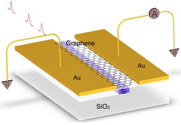
To address this, graphene has been integrated into nanocavities, microcavities, and plasmon resonators; yet, these approaches restrict photodetection to narrow bands. Hybrid graphene–quantum dot architectures can greatly improve responsivity, but at the cost of response speed. In this research project, a waveguide-integrated graphene photodetector was demonstrated that simultaneously exhibits high responsivity, high speed and broad spectral bandwidth.
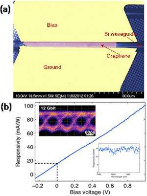
Using a metal-doped graphene junction coupled evanescently to the waveguide, the detector achieves a photoresponsivity exceeding 0.1 A/W together with a nearly uniform response between 1,450 nm and 1,590 nm. Under zero-bias operation, response rates exceeding 20 GHz were achieved, and an instrumentation-limited 12 Gbit/s optical data link was confirmed.
The responsivity is 0.1 A/W, which is comparable to current germanium photodetectors in silicon photonic integrated circuits. The response rates of the device exceed 20 GHz, such that the system performs without distortion in a real 12-Gbit/s optical data link. Further, this graphene light detector shows 16 times higher response than conventional graphene-based photodetectors. These characteristics have established the groundwork for on-chip graphene optoelectronics, which provides a promising solution for efficient on-chip optical networks.

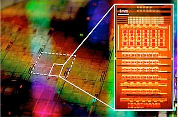
CFN Capabilities: The CFN Nanofabrication Facility was used to perform advanced fabrication processes that integrated graphene with silicon photonic integrated circuits.

More information: "Chip-Integrated Ultrafast Graphene Photodetector with High Responsivity." X. Gan, et al. Nature Photonics 7, 883-887 (2013) DOI: 10.1038/nphoton.2013.253
Journal information: Nature Photonics
Provided by Brookhaven National Laboratory


