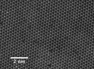
Scalable CVD process for making 2-D molybdenum diselenide

(Phys.org) —Nanoengineering researchers at Rice University and Nanyang Technological University in Singapore have unveiled a potentially scalable method for making one-atom-thick layers of molybdenum diselenide—a highly sought semiconductor that is similar to graphene but has better properties for making certain electronic devices like switchable transistors and light-emitting diodes.
The method for making two-dimensional molybdenum diselenide uses a technique known as chemical vapor deposition (CVD) and is described online in a new paper in the American Chemical Society journal ACS Nano. The finding is significant because CVD is widely used by the semiconductor and materials industries to make thin films of silicon, carbon fibers and other materials.
"This new method will allow us to exploit the properties of molybdenum diselenide in a number of applications," said study leader Pulickel Ajayan, chair of Rice's Department of Materials Science and NanoEngineering. "Unlike graphene, which can now easily be made in large sheets, many interesting 2-D materials remain difficult to synthesize. Now that we have a stable, efficient way to produce 2-D molybdenum diselenide, we are planning to expand this robust procedure to other 2-D materials."
In the Rice study, Ajayan and colleagues tested their atomically thin layers of molybdenum diselenide by building a field effect transistor (FET), a commonly used device in the microelectronic industry. Tests of the FET found the electronic properties of the molybdenum diselenide layers were significantly better than those of molybdenum disulfide; the latter is a similar material that has been more extensively studied because it was easier to fabricate. For example, the FET tests found that the electron mobility of Rice's molybdenum diselenide was higher than that of CVD-grown, molybdenum disulfide.
In solid-state physics, electron mobility refers to how quickly electrons pass through a metal or semiconductor in the presence of an electric field. Materials with high electron mobility are often preferred to reduce power consumption and heating in microelectronic devices.
"Being able to make 2-D materials in a controlled fashion really will make an impact on our understanding and use of their fascinating properties," said study co-author Emilie Ringe, assistant professor of materials science and nanoengineering and of chemistry at Rice. "Characterizing both the structure and function of a material, as we have done in this paper, is critical to such advances."
Molybdenum diselenide and molybdenum disulfide each belong to a class of materials known as transition metal dichalcogenides; TMDCs are so named because they consist of two elements, a transition metal like molybdenum or tungsten and a "chalcogen" like sulfur, selenium or tellurium.
TMDCs have attracted intense interest from materials scientists because they have an atomic structure similar to graphene, the pure carbon wonder materials that attracted the 2010 Nobel Prize in physics. Graphene and similar materials are often referred to as two-dimensional because they are only one atom thick. Graphene has extraordinary electronic properties. For example, its electron mobility is tens of thousands of times greater than that of TMDCs.
However, two-dimensional TMDCs like molybdenum diselenide have attracted intense interest because their electronic properties are complementary to graphene. For example, pure graphene has no bandgap—a useful electronic property that engineers can exploit to make FETs that are easily switched on and off.
As with many nanomaterials, scientists have found that the physical properties of TMDCs change markedly when the material has nanoscale properties. For example, a slab of molybdenum diselenide that is even a micron thick has an "indirect" bandgap while a two-dimensional sheet of molybdenum diselenide has a "direct" bandgap. The difference is important for electronics because direct-bandgap materials can be used to make switchable transistors and sensitive photodetectors.
"One of the driving forces in Rice's Department of Materials Science and NanoEngineering is the close collaborations that develop between the people who are focused on synthesis and those of us involved with characterization," said Ringe, who joined Rice's faculty in January. "We hope this will be the beginning of a series of new protocols to reliably synthesize a variety of 2-D materials."
More information: "Chemical Vapor Deposition Growth of Crystalline Monolayer MoSe." Xingli Wang , Yongji Gong , Gang Shi , Wai Leong Chow , kunttal Keyshar , Gonglan Ye , Robert Vajtai , Jun Lou , Zheng Liu , Emilie Ringe , Beng Kang Tay , and Pulickel M Ajayan. ACS Nano, Just Accepted Manuscript, DOI: 10.1021/nn501175k . Publication Date (Web): March 29, 2014
Journal information: ACS Nano
Provided by Rice University


