Graphene: Minor rotation of 'chicken wire' has major consequences

Since the discovery of graphene, a great future has been predicted for the material, which is strong and highly conductive. Just one carbon atom layer thick, graphene can lead to new electronics. Examples include printable and flexible electronics, touch screens and OLEDs. For this, interaction with other materials is necessary, however. PhD student Menno Bokdam from the University of Twente MESA+ Institute for Nanotechnology examined what happens at the interface with other materials and thus brings graphene electronics a step closer. He will defend his PhD thesis on 15 November.
Graphene was dubbed a 'miracle material' when Andre Geim and Konstantin Novoselov received the Nobel Prize for Physics for it in 2010. The carbon is extremely thin, has a chicken wire structure, and can conduct electrons very well. But how does it behave in contact with another material with a similar structure, such as boron nitride? What happens if the boron nitride layer is inserted between a layer of copper and a layer of graphene? Insight into the interfaces is critical if you want to design electronics.
'Gap' or not?
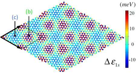
Bokdam has performed detailed electron structure theory calculations of graphene on boron nitride. This material is also very thin and has almost exactly the same chicken wire structure, but differs from graphene because it does not conduct electricity. Placed on top of one another, a redistribution of electrons in the graphene can be seen. This creates a pattern of electrons and 'holes', like a kind of moiré pattern that is also seen when two bars slide over one another. If the angle between the two mesh structures is precisely chosen, a 'gap' is also revealed: a gulf between occupied and unoccupied energy states. An electron must overcome that gulf to conduct electricity: a defining characteristic for a semiconductor. There is a worldwide debate about whether the 'gap' exists or not: a previous MESA+ publication on this subject is one of the institute's most cited documents. Bokdam now proposes that the gap does not arise when graphene and boron nitride are laid on top of one another at a random angle, but does arise when they are precisely rotated relative to one another.
External world
What if the combination of graphene/boron nitride is applied on copper for contact with the external world? In that case, a charge distribution, a so-called dipole layer, is also formed on the interface between copper and boron nitride. Because the boron nitride layer is ultra-thin, the charge is able to 'tunnel' through the boron nitride, although it does not conduct electricity. The dipole layer has a major influence on the number of tunneling electrons. By choosing a suitable metal and applying an electric field, the concentration of charge carriers in graphene and thus the conduction through the graphene can be influenced.
He has thus developed an understanding of the interaction between different two-dimensional materials and with metals. The findings are important for designing electronic components based on the graphene and other 2D materials.
Provided by University of Twente


