Researchers develop thin film semiconductor that will drive production of next-generation displays

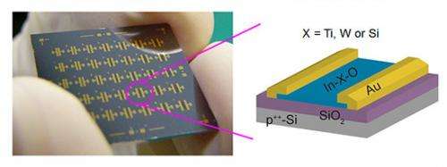
Researchers at the National Institute for Materials Science have developed a pixel switching semiconductor, which will be the key to driving next-generation displays, by using an oxide film with a new elemental composition.
A flat panel display is an important interface in modern information society, which displays the electronic bit information used in machines in a human-recognizable form. Conventionally, amorphous silicon thin films and polysilicon thin films had been used to make field-effect transistors to be used as pixel switches for TVs and smartphones, but there have been strong calls for the development of high-performance semiconductor films with higher definition or higher speed. At present, indium gallium zinc oxide (IGZO) transistors are potential oxide semiconductors with high field-effect mobility. However, it is generally difficult to adjust the manufacturing conditions for stably and efficiently producing high-performance oxide semiconductors, and this is presenting a major challenge in actual production.
Therefore, materials that can adapt to broader manufacturing conditions are hoped to be developed for thin-film formation.
We added an infinitesimal amount of metal oxide (titanium oxide, tungsten oxide, silicon oxide, etc.) to indium oxide, and found a factor that decides the film deposition conditions for a thin film to behave as a semiconductor, for the first time in the world.
When an oxide film contains metal with low bond dissociation energy, the thin film absorbs or desorbs oxygen easily and the conductivity of the film changes. For example, zinc has very low bond dissociation energy, so a thin film using zinc absorbs or desorbs oxygen easily when heated or cooled. This finding suggests that the manufacturing conditions for oxide semiconductors can be controlled by focusing on the bond dissociation energy. In fact, we confirmed that film deposition conditions can be broadened by adding silicon oxide with high bond dissociation energy to indium oxide. We also confirmed stabilization of thin-film conductivity in post-deposition heat treatment.
The research results are expected to be effective not only for reducing the power consumption of displays which consume about half of the power in rapidly diffusing smartphones, but also for achieving higher frequencies to realize higher-definition TVs. Moreover, the thin film developed in this research contributes to conserving precious resources by not using zinc, which is a trace element of concern, or high-cost gallium which is used in large quantities for galvanized steel sheets or as a rubber vulcanizing agent, while it also enables the manufacture of flat panel displays not affected by wild fluctuations in raw material prices.
The research results will be published in the online edition of the U.S. applied physics journal, Applied Physics Letters, in the near future.
Journal information: Applied Physics Letters
Provided by National Institute for Materials Science


