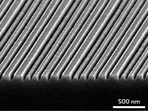
Method that boosts contrast of high-resolution optical images has potential to enable lithography at the nanoscale

When looking to produce the tiny semiconductor components used in electronic devices, photolithography is the process of choice. It not only provides high-resolution images, but also allows high-throughput production. However, as miniaturization of electronic circuits advances unceasingly, traditional photolithography hits both fundamental and cost limits. Now, a new photolithographic technique that will produce features smaller than those possible today is on the horizon. This development is thanks to an international research team led by Jing Hua Teng and Hong Liu from the A*STAR Institute of Materials Research and Engineering, Singapore, which included co-workers from the A*STAR Data Storage Institute, Singapore.
In traditional photolithography, light is used to write, for example, the layout of an electronic circuit onto a substrate coated with a light-sensitive material. The assembly is then chemically processed in a way that makes the desired pattern appear on the final component. The minimum size of the features that can be produced with this method is given by the optical diffraction limit: the resolution that can be obtained in optical images cannot be higher than about half of the wavelength of the light used. This limit is typically on the order of several hundreds of nanometers. And, with a view to further miniaturization of electronic components, it constitutes a genuine roadblock, explains Teng.
Physicists have proposed several methods to beat the diffraction limit, including the use of so-called superlenses. The resolution of superlens images exceeds the diffraction limit; however, these images tend to suffer from poor contrast, and this has limited their usefulness for lithography.
Teng and his co-workers demonstrated that they could produce superlens images with a resolution below 50 nanometers and a contrast sufficient for photolithographic purposes. The trick was to carefully control the surface of the lens, which consists of a thin silver film. "A smooth surface ensures that very little light is lost due to scattering," explains Teng. Through careful optimization of the fabrication process, he and his team succeeded in producing silver superlenses with imperfections that were less than 2 nanometers in height.
The team's next goal is to optimize the lithography process and the materials involved to meet the high-throughput requirements for industry-scale applications. The result should be a versatile tool for optical lithography in the nano-regime. "Superlens lithography is a promising technology for next-generation optical nanolithography for the semiconductor industry, but also for bioengineering and data storage," says Liu.
More information: Liu, H., Wang, B., Ke, L., Deng, J., Choy, C. C. et al. High contrast superlens lithography engineered by loss reduction. Advanced Functional Materials 22, 3777–3783 (2012). onlinelibrary.wiley.com/doi/10 … m.201200788/abstract
Journal information: Advanced Functional Materials


