November 2, 2012 feature
New two-dimensional semiconductor has ideal band gap for solar harvesting

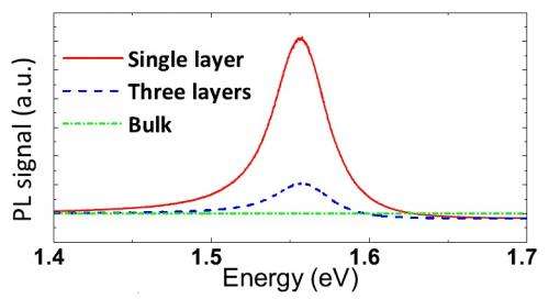
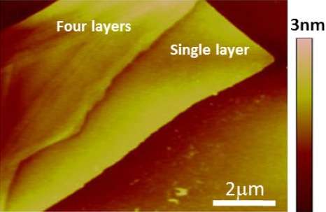
(Phys.org)—At its heart, photovoltaics research is about finding materials with specific properties that make them good at absorbing sunlight and converting it into electricity. The best photovoltaics materials are semiconductors that have optimal band gap values ranging from 1-1.6 eV, allowing them to absorb particular portions of the solar spectrum depending on the value of the band gap. In a new study, materials scientists have synthesized and characterized a new semiconductor material that consists of an atomically thin (0.7-nm) layer of selenium and molybdenum that has an ideal band gap for solar harvesting and optoelectronics applications, and also exhibits some unique behavior.
The researchers, a team from the University of California, Berkeley; MIT; and the Chinese Academy of Sciences, have published their study in a recent issue of Nano Letters.
"Here, we have isolated single layers of molybdenum diselenide (MoSe2) and shown their promising band gap value of 1.5 eV for solar harvesting and possibly other optoelectronics applications," coauthor Junqiao Wu, a professor at the University of California, Berkeley, told Phys.org. "According to the Shockley-Queisser limit for the theoretical maximum efficiency of solar cell semiconductors, semiconductors with band gaps between 1 and 1.6 eV have the greatest potential to form an efficient cell. This is because a wider band gap would be unable to absorb low-energy photons (and thus photocurrent would be low), and a narrower band gap would lose too many high-energy photons to heat (and thus photovoltage would be low). We are within this range in the single-layer limit."
In addition to its appealing band gap, MoSe2 is also attractive because of another unusual property: it has almost degenerate direct and indirect band gaps in the few-layer limit, i.e., the direct and indirect band gaps have almost the same energy in the few-layer limit. Although materials with both direct and indirect band gaps can absorb photons whose energy is near the band gap energy, materials with direct band gaps don't allow photons to penetrate as far, which makes them better (and usually thinner) light absorbers than materials with indirect band gaps.

MoSe2, like most other transition-metal chalcogenides, has an indirect band gap in bulk form and a direct band gap as a two-dimensional single layer. Typically, in order to transform the indirect band gap to a direct band gap, a single layer must be physically isolated from a piece of bulk material.
In the new study, the researchers found that they could switch the indirect band gap in a few-layered piece of MoSe2 to a direct band gap simply by increasing the temperature. As the researchers explain, increasing the temperature to 100 °C (212 °F) causes the multiple layers of the material to thermally decouple from each other due to thermal expansion of the space between layers. Essentially, the multiple layers each act as individual layers with direct band gaps. Decoupling lifts the degeneracy so the material becomes more direct band and more luminescent.
Since many transition-metal chalcogenides possess an indirect band gap in bulk form and become direct as a single layer, it might be expected that other materials could also have their band gaps switched by changing the temperature. However, when the scientists tested a similar material, molybdenum disulfide (MoS2), they found that, even though increasing the temperature expanded the interlayer distance as it did in MoSe2, its band gap remained indirect in the few-layer form, unlike in the case of MoSe2.
This difference is due to MoSe2 having a smaller difference (about half) between the values of its indirect band gap and direct band gap compared with that of MoS2. A larger energy difference for MoS2 means that its band gap is far from degenerate and its layers cannot be thermally decoupled from the optical point of view; the only way to change the band gap to direct would be to physically isolate a single layer from the bulk.
So far, it seems that MoSe2 is the only material that changes its band gap type due to a change in temperature. However, the researchers think that there are other two-dimensional materials with almost degenerate indirect and direct band gap values that may behave in a similar way.
"MoSe2 is special in the sense that its indirect and direct band gap values are already close in value, and a small increase in temperature was enough to slightly decouple the layers from each other and push it towards the direct band gap regime," said coauthor Sefaattin Tongay of the University of California, Berkeley.
The ability to control the band gap of MoSe2, along with its attractive 1.5 eV direct band gap in single-layer form, makes the material appealing for applications including solar energy conversion in single-junction solar cells, LEDs, optoelectronic devices, and photoelectrochemical cells. MoSe2 membranes may also be used to functionalize the surface of other materials to form efficient solar harvesting structures.
"Currently, we are designing functional two-dimensional semiconductors and scouting what these materials can offer," Tongay said. "We want to find applications and explore new physics in reduced dimensions."
More information: Sefaattin Tongay, et al. "Thermally driven crossover from indirect toward direct bandgap in 2D semiconductors: MoSe2 versus MoS2." Nano Letters. DOI: 10.1021/nl302584w http://pubs.acs.org/doi/abs/10.1021/nl302584w
Journal information: Nano Letters
Copyright 2012 Phys.org
All rights reserved. This material may not be published, broadcast, rewritten or redistributed in whole or part without the express written permission of PhysOrg.com.


.jpg)


