October 2, 2012 report
Researchers glimpse the inside of a photonic crystal

(Phys.org)—While today's smart phones, tablets, and other small electronic devices rely on electrical data connections, in the future they may use optical connections in order to become even faster and smaller. Photonic crystals are ideal tools for this purpose, since they can guide and bend light on the nanometer scale. So far, researchers have not been able to look inside photonic crystals to measure how the light intensity is distributed. Now in a new study, a team of researchers from the MESA+ Institute at the University of Twente, The Netherlands, has developed a method that can measure the intensity distribution of light inside photonic crystals.
The study, which is published in a recent issue of Optics Express, may lead to new insights into photonic crystals that could assist in the development of new applications.
As the researchers explain, photonic crystals are materials with an intricate three-dimensional structure that manipulates light in ways similar to how semiconductors control electrons. Photonic crystals have a periodic structure with a length scale on the order of the wavelength of light. An example of a photonic crystal found in nature is the gem opal, which consists of a regular array of tiny silicate spheres that are ordered like atoms in a crystal lattice, but on a length scale a thousand times larger than the atoms in a photonic crystal.
A major goal in this area of research is to make photonic crystals interact with light strongly enough to achieve a "photonic band gap," which is a range of light colors that are prevented from propagating in any direction. Band gaps can result from disorder in a crystal, since disorder leads to localized states that effectively trap light in a cage. This type of control can allow researchers to harness light beams and steer them around tiny optical chips.
In order to control light in this way, it's helpful to know the electromagnetic field distribution inside the photonic crystals. So far, the only optical method to map local fields is near-field scanning optical microscopy, which scans the surface of the crystal. However, this technique has several drawbacks because it cannot probe the fields inside the crystal, whereas the new method presented here can.
"We have demonstrated for the first time how to look into the inside of photonic crystals," lead author Thomas Denis of the University of Twente told Phys.org. "With an astonishingly simple method we were able to map the absolute strength of an individual field component inside a photonic crystal. Such a method should be of high importance for the design of novel photonic crystal devices, such as fast optical interconnects on computer chips."
To map the strength of the electromagnetic field at different locations inside photonic crystals, the researchers set up an experiment in which they placed a photonic crystal between two aluminum mirrors. Inside the cavity, light bounces back and forth between the mirrors. Since light is a wave, only waves whose wavelengths fit the length of the cavity can build up. In other words, only a specific color can exist inside the cavity.
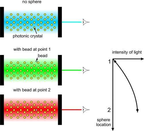
After measuring the crystal's resonating color, or frequency, the researchers then investigated how the frequency would be altered when they lowered a 2-mm bead hanging from a nylon string inside the crystal. The bead scatters nearby electromagnetic waves, changing the crystal's frequency in a way that is proportional to the light intensity at that location. By measuring the frequency shift when moving the bead to various locations, the researchers could map the electromagnetic field strength throughout the inside of the photonic crystal.
"For example, in the figure above, the cavity limits the build-up of light to blue light," Denis said. "When placing the bead inside the photonic crystal, this leads to scattering, which changes the light color that resonates in the cavity. The waves have to make a small detour around the scattering object. Therefore, the color where the light resonates is changed, which can be measured. In the figure it varies from green to red depending on the position of the bead. By moving the bead throughout the cavity, this allows us to map the light intensity at all locations by measuring the resulting color shift."
The researchers also explained that the electric field inside the photonic crystal has six components, and each of these components can be measured separately by choosing a bead with a suitable material, shape, and orientation so that only one component contributes to the frequency shift.
In the future, the researchers also want to perform modified experiments, such as placing the bead on a carbon nanotube acting as the string. An atomic force microscope could control the nanotube's position and provide high spatial resolution of the field inside the crystal. Ultimately, the ability to map the inside of a photonic crystal provides a valuable tool for using these devices in future applications.
More information:
T. Denis, B. Reijnders, J. H. H. Lee, P. J. M. van der Slot, W. L. Vos and K.-J. Boller. "Mapping individual electromagnetic field components inside a photonic crystal." Optics Express, Vol. 20, Issue 20, pp. 22902-22913 (2012) DOI: 10.1364/OE.20.022902
Also at arXiv:1207.2004 [physics.optics]
Journal information: Optics Express
© 2012 Phys.org


