Another advance on the road to spintronics: Researchers unlock ferromagnetic secrets of promising materials

(Phys.org)—Spintronic technology, in which data is processed on the basis of electron "spin" rather than charge, promises to revolutionize the computing industry with smaller, faster and more energy efficient data storage and processing. Materials drawing a lot of attention for spintronic applications are dilute magnetic semiconductors – normal semiconductors to which a small amount of magnetic atoms is added to make them ferromagnetic. Understanding the source of ferromagnetism in dilute magnetic semiconductors has been a major road-block impeding their further development and use in spintronics. Now a significant step to removing this road-block has been taken.
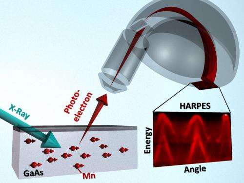
A multi-institutional collaboration of researchers led by scientists at the U.S. Department of Energy's Lawrence Berkeley National Laboratory (Berkeley Lab), using a new technique called HARPES, for Hard x-ray Angle-Resolved PhotoEmission Spectroscopy, has investigated the bulk electronic structure of the prototypical dilute magnetic semiconductor gallium manganese arsenide. Their findings show that the material's ferromagnetism arises from both of the two different mechanisms that have been proposed to explain it.
"This study represents the first application of HARPES to a forefront problem in materials science, uncovering the origin of the ferromagnetism in the so-called dilute magnetic semiconductors," says Charles Fadley, the physicist who led the development of HARPES. "Our results also suggest that the HARPES technique should be broadly applicable to many new classes of materials in the future."
Fadley, who holds joint appointments with Berkeley Lab's Materials Sciences Division and the University of California (UC) Davis where he is a Distinguished Professor of Physics, is the senior author of a paper describing this work in the journal Nature Materials. The paper is titled "Bulk electronic structure of the dilute magnetic semiconductor GaMnAs through hard X-ray angle-resolved photoemission." The lead and corresponding author is Alexander Gray, formerly with Fadley's research group and now with the Stanford University and the SLAC National Accelerator Laboratory.

For the semiconductors used in today's computers, tablets and smart phones, etc., once a device is fabricated it is the electronic structures below the surface, in the bulk of the material or in buried layers, that determine its effectiveness. HARPES, which is based on the photoelectric effect described in 1905 by Albert Einstein, enables scientists to study bulk electronic effects with minimum interference from surface reactions or contamination. It also allows them to probe buried layers and interfaces that are ubiquitous in nanoscale devices, and are key to smaller logic elements in electronics, novel memory architectures in spintronics, and more efficient energy conversion in photovoltaic cells.
"The key to probing the bulk electronic structure is using hard x-rays, which are x-rays with sufficiently high photon energies to eject photoelectrons from deep beneath the surface of a solid material," says Gray, who worked with Fadley to develop the HARPES technique. "High-energy photons impart high kinetic energies to the ejected photoelectrons, enabling them to travel longer distances within the solid. The result is that more of the signal originating from the bulk will be detected by the analyzer."
In this new study, Gray and Fadley and their collaborators, used HARPES to shed important new light on the electronic bulk structure of gallium manganese arsenide (GaMnAs). As a semiconductor, gallium arsenide is second only to silicon in widespread use and importance. If a few percent of the gallium atoms in this semiconductor are replaced with atoms of manganese the result is a dilute magnetic semiconductor. Such materials would be especially well-suited for further development into spintronic devices if the mechanisms behind their ferromagnetism were better understood.

"Right now the temperature at which gallium manganese arsenide operates as a dilute magnetic semiconductor is 170 Kelvin," Fadley says. "Understanding the actual mechanism by which the magnetic moments of individual manganese atoms are coupled so as to become ferromagnetic is critical to being able to design future materials that would operate at room temperature."
The two prevailing theories behind the origin of ferromagnetism in GaMnAs and other dilute magnetic semiconductors are the "p-d exchange model" and the "double exchange model." According to the p-d exchange model, ferromagnetism is mediated by electrons residing in the valence bands of gallium arsenide whose influence extends through the material to other manganese atoms. The double exchange model holds that the magnetism-mediating electrons reside in a separate impurity band created by doping the gallium arsenide with manganese. These electrons in effect jump back and forth between two manganese atoms so as to lower their energy when their ferromagnetic magnets are parallel.
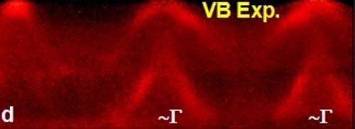
"Our bulk-sensitive HARPES measurements revealed that the manganese-induced impurity band is located mostly between the gallium arsenide valence-band maximum and the Fermi level, but the manganese states are also merged with the gallium arsenide valence bands," Gray says. "This is evidence that the two mechanisms co-exist and both act to give rise to ferromagnetism."
Adds Fadley, "We now have a better fundamental understanding of electronic interactions in dilute magnetic semiconductors that can suggest future materials with different parent semiconductors and different magnetic dopants. HARPES should provide an important tool for characterizing these future materials."
Gray and Fadley conducted this study using a high intensity undulator beamline at the SPring8 synchrotron radiation facility in Hyogo, Japan, which is operated by the Japanese National Institute for Materials Sciences. New HARPES studies are now underway at Berkeley Lab's Advanced Light Source (ALS) using the Multi-Technique Spectrometer/Diffractometer endstation at the hard x-ray photoemission beamline (9.3.1).
More information: Co-authoring the Nature Materials paper with Gray and Fadley were Jan Minár, Shigenori Ueda, Peter Stone, Yoshiyuki Yamashita, Jun Fujii, Juergen Braun, Lukasz Plucinski, Claus Schneider, Giancarlo Panaccione, Hubert Ebert, Oscar Dubon and Keisuke Kobayashi.
Journal information: Nature Materials
Provided by Lawrence Berkeley National Laboratory


