September 24, 2012 weblog
Uh-oh, Intel. Globalfoundries to fast-forward into 14nm
(Phys.org)—Globalfoundries has made an announcement that amounts to a direct challenge to Intel, in the latter's race to get further ahead in the mobile device ecosystem. Both Globalfoundries and Intel will be racing for a more dominant position with higher performing and power efficient systems for smartphones and other devices. In short, Globalfoundries announced Thursday that it is accelerating its technology roadmap. Its newest design achievement for the mobile market is in the form of 14nm chip technology. The company provided some details about its 14nm-XM ("extreme mobility") process.
This is a nonplanar architecture optimized for low-power, mobile system-on-chip (SoC) designs. These chips will deliver a 40 percent to 60 percent improvement in battery life compared to two-dimension planar transistors at the 20nm node.
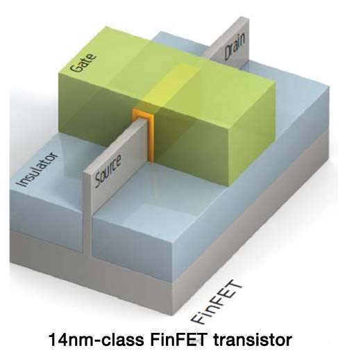
Globalfoundries will go "3-D" in the use of three-dimensional "FinFET" transistors. The big deal about "FinFET" rests in its promoted superior low-power attributes. The FinFET architecture takes a traditional two-dimensional transistor design and turns the conductive channel on its side, resulting in a three-dimensional fin structure, surrounded by a gate controlling the flow of current.

The 3-D transistor design operates at a lower voltage with minimal current leakage. This leads to a longer battery life for mobile applications and less power consumption for plugged-in applications. The power-consumption advantage could have important implications for networking chips in data centers.
Intel's challenge is not only in the rival company's technology but also in 14nm timelines. Globalfoundries is speeding up its timeline for its 14nm process. Chip watchers note that in so doing it is playing leapfrog over other companies.
The company will be ready to roll with a 14-nanometer process that will include its three-dimensional transistor architecture. This is said to be similar to Intel's Tri-Gate method. Enthusiasts say that the 14nm-XM design is expected to carry performance and power benefits of three-dimensional FinFET transistors, possibly influencing a newer generation of mobile devices.
With the Globalfoundries plan, chip designers will be able to start producing sample 14 nanometer chips in 2013. In 2014 or early 2015, the 14 nm chips will be part of the consumer marketplace. Technology development of the 14nm-XM has begun in Globalfoundries' Fab 8, a fabrication plant in Saratoga County, New York. The company is making early process design kits (PDKs) which are available now. Customer tape-outs—the final result of the design—are expected in 2013.
Globalfoundries was formerly a manufacturing arm of AMD. Headquartered in Milpitas, California, Globalfoundries now counts itself as one of the largest foundries in the world by revenue.
More information: www.globalfoundries.com/technology/14XM.aspx
© 2012 Phys.org


