New design reduces the areal footprint of nanowire transistors by a factor of two

Semiconductor chip makers first began the production of three-dimensional (3D) transistors in 2011. Engineers can pack more 3D transistors onto a single chip because they are much more compact than traditional transistors.
For future generations of semiconductor chips, however, there is a need to shrink these 3D transistors further and the use of vertical nanowires in the transistor design is one of the promising approaches. Moreover, the area taken up by a nanowire-based transistor is typically half that of a planar transistor — or even less if considering more complicated components, like inverters. Xiang Li at the A*STAR Institute of Microelectronics and co-workers have now integrated two transistors onto a single vertical silicon nanowire, pushing the areal density limit of nanowire transistors even further.
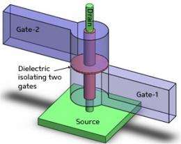
The researchers used wrap-around gates, or ‘gate-all-around’ gates, in the making of their device. These gates consist of a vertical cylinder, at the center of which lies the nanowire. They are much better at controlling the transistor current than traditional planar gates. Li and co-workers decreased the area required for a gate-all-around nanowire transistor by a factor of two by constructing two transistors out of a single vertical nanowire. Their design involves two wrap-around gates, one above the other, separated by a thin dielectric layer to isolate them electrically (see image). Unlike other independent double-gate transistor designs, such as those employing a vertical fin-like channel, changing the gate voltage applied to one transistor does not change the threshold (or turn-on) voltage of the other. This means that either of the gates can modulate the nanowire current independently.
As a result, Li and co-workers were able to construct a simple logic device using just one nanowire. For a nanowire doped with negative carriers, current was able to flow when both gate voltages were high, but current stopped when either gate voltage was low. This device therefore functioned as an ‘AND’ digital gate, but used only half the area it otherwise would require. The stacked gate arrangement may also be useful for enabling an emerging type of transistor, called a tunnel field effect transistor (TFET). Because TFETs rely on the tunneling of electrons across a barrier rather than the thermal activation of electrons, they turn on very quickly and consume very little power. Li says the tunnel junction required for a TFET could be formed between the two gates of the dual-gate nanowire geometry, allowing a particularly compact implementation. The dual-gate design could also be used for other technologies, such as non-volatile memory.
More information: Li, X. et al. Vertically stacked and independently controlled twin-gate MOSFETs on a single Si nanowire. IEEE Electron Device Letters 32, 1492–1494 (2011).


