March 6, 2009 feature
Nanochemistry in Action

(PhysOrg.com) -- Using a single-walled carbon nanotube (SWCNT) as a test tube, scientists can explore chemistry at the nanoscale, which involves some unique effects. Nanotubes provide a confined, one-dimensional space in which to isolate molecules, allowing nanoscale confinement effects to influence the chemical reactions.
In a recent study, a team of scientists from the UK, Austria, Germany and Japan have experimented with nano test tube chemistry by performing electron doping of carbon nanotubes using cerium compounds. Doping provides a promising means of tuning the nanotubes’ bulk electronic properties. In addition to helping scientists understand nanoscale chemistry, these experiments also highlight the potential of using nanotubes in future electronic devices.
“We used nano test tube chemistry to functionalize the electronic properties of carbon nanotubes,” lead author of the study Hidetsugu Shiozawa of the University of Surrey told PhysOrg.com. “This allowed us to observe a fundamental physical phenomenon in bulk carbon nanotubes associated with a transition from semiconducting tubes to metallic.”
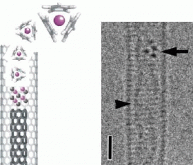
In their experiments, the researchers sealed a combination of carbon nanotube material and cerium organometallic compounds in a Pyrex tube, and annealed them at temperatures of up to 200°C (392°F). After annealing, the researchers observed SWCNTs containing cerium molecules. Further annealing at 1000°C (1832°F) in vacuum allowed the researchers to transform the filled SWCNTs into double-walled carbon nanotubes containing cerium (Ce@DWCNT). The transmission electron micrographs show sharp lines, which are original nanotubes, inside of which are parallel lines and dark dots, which are inner tubes and cerium ions, respectively.
The scientists were then able to extract electronic information from the cerium compounds in order to investigate the structures’ electronic properties. By measuring the energy of the emitted electrons using a method called resonance photoemission spectroscopy, the researchers found that the nanotube bundles had an increased density of conduction electrons after cerium doping, due to the transformation of the originally semiconducting nanotubes into metallic nanotubes.
“When chemistry is performed in these nano test tubes, the reactions that occur get closer to a result of a single molecule reacting with another, instead of billions of molecules reacting with each other and with anything else we put into laboratory test tubes,” said Shiozawa. “The one-dimensionally quantized electronic states of carbon nanotubes allow specific molecules and compounds to interact, so we can monitor the encapsulated chemical reactions through the carbon nanotubes’ electronic states.”
Overall the experiments showed how a nanoscale chemical reaction of cerium compounds can increase the conductivity of the surrounding carbon nanotubes. By using nanochemistry to controllably alter the nanotubes’ electric properties, researchers may be a step closer to using nanotubes for electronics applications.
“Our nano test tube chemistry allows a clean, slow and defined growth of carbon nanotubes,” said Shiozawa. “Individual chemistry events can be observed at the elemental level when materials are confined within the nano test tube. This nanochemistry process can be applied for studying the growth mechanism of carbon nanotubes. Its conceptual advance would be for any chemical reactions in general. We showed that doping of the host carbon nanotube can be varied via encapsulations and chemical reactions of molecules. This process might be applied for modulating electrical properties of a SWCNT at the nanoscale and provides for better compatibility of carbon nanotubes with electronics.”
Professor Ravi Silva, Director of the Advanced Technology Institute, added, “Our results are world-leading and will tell researchers and technologists working on the next generation of nanoelectronic devices some of the fundamental issues that must be taken into account in their design. We have shown that single atoms stuck on the surface of a carbon nanotube can have a tremendous effect on its electrical characteristics. The implications are widespread because these tubes are proposed to be used as wires in nano-scale integrated circuit chips within the next decade.”
The study is published in a recent issue of Physical Review Letters, and the research was sponsored by a Portfolio Partnership award by the Engineering and Physical Sciences Research Council (EPSRC), UK.
More information: H. Shiozawa, T. Pichler, C. Kramberger, M. Rümmeli, D. Batchelor, Z. Liu, K. Suenaga, H. Kataura, and S. R. P. Silva. Screening the missing electron: Nanochemistry in action, Physical Review Letters 102, 046804 (2009). link.aps.org/abstract/PRL/v102/e046804
Copyright 2009 PhysOrg.com.
All rights reserved. This material may not be published, broadcast, rewritten or redistributed in whole or part without the express written permission of PhysOrg.com.


