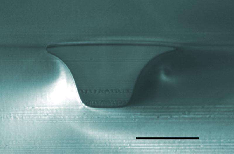
Technique to measure volumes of key 'Lab on a Chip' components

Imagine shrinking tubes and beakers—in fact, most of a clinical chemistry lab—down to the size of a credit card. When engineers figured out how to do that two decades ago, they enabled complex tests to be performed with tiny "lab on a chip" technology. But until now, there has been no way to accurately measure the size of the tiny vessels they created. Now,scientists at the National Institute of Standards and Technology have found a potential solution to this longstanding manufacturing issue.
The NIST approach could meet an important need in the microfluidics industry, which creates devices useful in fields from medical testing to toxin detection. It could be particularly important for miniaturized devices that rely on volume measurements to report, for example, the concentration of a particular molecule in a mixture.
Because microfluidic devices are good at straining and purifying liquids, they have found use across the biotech field, where they are invaluable for DNA testing, distilling specific proteins from a mixture, and other applications where a great number of samples need to be analyzed quickly. These labs on a chip can take a variety of shapes depending on their purpose, but they often feature tiny pipes and chambers where fluid samples flow and collect.
These channels and reservoirs have presented a longstanding problem to manufacturers, whose devices are often made of plastic. There's been no way to measure their dimensions effectively for quality control. It's hard for a company that makes plastic devices to guarantee that one of their miniature labs will perform the same as another—or to design devices whose function depends on knowing how much fluid there is and how much difference there is between the intended design and the final assembly.
"The inability to determine these dimensions limits a multi-billion dollar industry," says NIST's Darwin Reyes. "Without them, your chip might not give you the right value for the concentration of insulin in a blood test, for example, or tell you how much DNA there was at one crucial step in the process."
The NIST team's solution has been to survey a number of potential measurement methods in the hopes that some combination of them would turn out to deliver reliable results. According to Reyes, it was the first time anyone had looked at multiple techniques and compared their efficacy quantitatively for knowing the actual dimensions of the channel.
Their survey led them to a pair of techniques: optical coherence tomography (OCT) and confocal microscopy (CM). They found that while neither could reliably measure all dimensions by itself, OCT could measure a channel's depth to an accuracy of 4 percent while CM gave readings of its width at the bottom to within 5 percent. The results matched those obtained by filling the channels with epoxy and measuring its cross-section later—"an approach that gives great answers but unfortunately ruins the device in the process," Reyes says.
The combination of OCT and CM only takes a few minutes and would therefore be fast enough to meet manufacturers' needs, Reyes says, though at this point it would be expensive. But, he says, the work "opens the door for what could be seen as a standard method for measuring microfluidic devices in very little time and with traceable accuracy and precision."
More information: "Dimensional metrology of lab-on-a-chip internal structures: A comparison of optical coherence tomography with confocal fluorescence microscopy." Journal of Microscopy, published online April 8, 2015. DOI: 10.1111/jmi.12245
Provided by National Institute of Standards and Technology


