June 10, 2011 report
IBM creates first graphene based integrated circuit

(PhysOrg.com) -- Taking a giant step forward in the creation and production of graphene based integrated circuits, IBM has announced in Science, the fabrication of a graphene based integrated circuit on a single chip. The demonstration chip, known as a radio frequency "mixer" is capable of producing frequencies up to 10 GHz, and demonstrates that it is possible to overcome the adhesion problems that have stymied researchers efforts in creating graphene based IC's that can be used in analog applications such as cell phones or more likely military communications.
IBM and others had previously demonstrated that it was possible to create a graphene based transistor; this latest research takes that technology one step further by marrying the transistor and other electronics on a single chip to create a full-fledged integrated circuit.
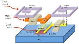
The graphene circuits were started by growing a two or three layer graphene film on a silicon surface which was then heated to 1400°C. The graphene IC was then fabricated by employing top gated, dual fingered graphene FET’s (field-effect transistors) which were then integrated with inductors. The active channels were made by spin-coating the wafer with a thin polymer and then applying a layer of hydrogen silsequioxane. The channels were then carved by e-beam lithography. Next, the excess graphene was removed with an oxygen plasma laser, and then the whole works was cleaned with acetone. The result is an integrated circuit that is less than 1mm2 in total size.
The chip produces output signals with mixed frequencies, hence its name, and while the prototype developed is not expected to be used in an actual device, future chips using the new technology are expected to be used in wireless communications. Since a major source of the funding for the research has been provided by the U.S. Defense Advanced Research Projects Agency (DARPA) the first uses of such a chip in an application is likely to be for secretive communications between airborne military pilots; the ultra high frequencies generated make it ideal for such secure applications.
Getting the graphene to adhere to other electronic components was by all accounts the most difficult part of the whole process, and apparently took the team, led by Phaedon Avouris, all of a year to accomplish; but it was clearly well worth the effort as research teams the world over continue to search for an eventual replacement to silicon in integrated chips, which by most accounts will hit its limits within the next few years.
More information: Wafer-Scale Graphene Integrated Circuit, Science 10 June 2011: Vol. 332 no. 6035 pp. 1294-1297. DOI: 10.1126/science.1204428
ABSTRACT
A wafer-scale graphene circuit was demonstrated in which all circuit components, including graphene field-effect transistor and inductors, were monolithically integrated on a single silicon carbide wafer. The integrated circuit operates as a broadband radio-frequency mixer at frequencies up to 10 gigahertz. These graphene circuits exhibit outstanding thermal stability with little reduction in performance (less than 1 decibel) between 300 and 400 kelvin. These results open up possibilities of achieving practical graphene technology with more complex functionality and performance.
© 2010 PhysOrg.com


