Mapping deformation in buried semiconductor structures using the hard X-Ray nanoprobe

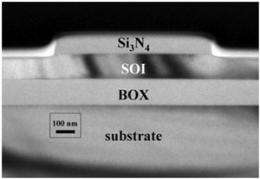
(PhysOrg.com) -- Scientists from IBM's T. J. Watson Research Center and Columbia University, working with the X-Ray Microscopy Group, have mapped rotation and strain fields across a silicon-on-insulator (SOI) structure that included a liner of stressed Si3N4 using X-ray nanodiffraction (nano-XRD) at the CNM/APS Hard X-Ray Nanoprobe beamline.
Inducing strain in semiconductors is an important method to improve performance of complementary metal-oxide semiconductor (CMOS) devices. One strategy for inducing strain includes the deposition of liner materials that possess residual stress, ultimately producing strain within the CMOS device. However, this strain is heterogeneous at the nanoscale, leading to a wide distribution of environments along current-carrying paths of the structure. Improved understanding of the distribution of strain in CMOS devices is critical for continued improvement of their efficiency. Although a number of techniques have been applied to characterize strain at the nanoscale, none enable the mapping of subsurface regions or buried layers with the high spatial resolution offered by nano-XRD.

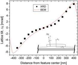
The new in situ studies reveal the distribution of lattice tilt as a function of position within the structure and also the maximum magnitude of the lattice tilt. The work is significant because it is one of the first nondestructive studies of subsurface strain with spatial resolution better than 100 nm done without sectioning or otherwise modifying the sample.
Modeling is also performed via a boundary element approach. The modeling and experimental results show that strain transfer into the underlying SOI from the liner primarily induces elastic deformation with secondary nanoscale regions exhibiting a unique noncontinuum, nonelastic response that is the subject of further study.
The Hard X-Ray Nanoprobe beamline is jointly managed by the CNM and the X-Ray Science Division of the Advanced Photon Source at Argonne National Laboratory.
More information: C. E. Murray et al., “Nanoscale silicon-on-insulator deformation induced by stressed liner structures,” J. Appl. Phys. 109, 083543 (2011). DOI:10.1063/1.3579421
Provided by Argonne National Laboratory


